Semiconductor device and method for manufacturing the same
A semiconductor and device technology, applied in the field of semiconductor devices and their manufacturing, to achieve the effect of high conduction breakdown voltage
- Summary
- Abstract
- Description
- Claims
- Application Information
AI Technical Summary
Problems solved by technology
Method used
Image
Examples
no. 1 example
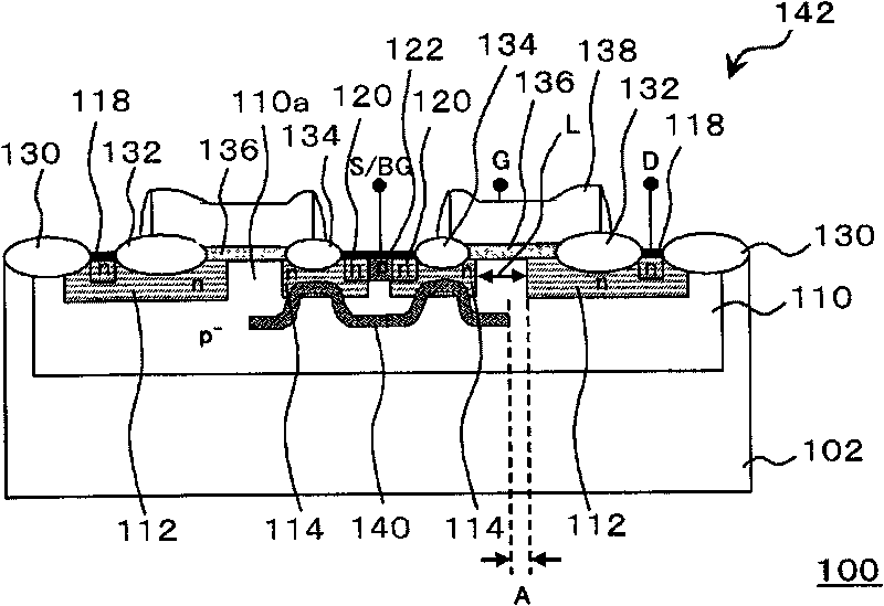
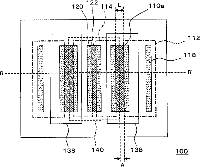
[0052] figure 1 is a cross-sectional view of the configuration of a semiconductor device according to an embodiment of the present invention. figure 2 is showing figure 1 A plan view of the configuration of the semiconductor device shown. figure 1 corresponds to along figure 2 The cross-sectional view taken along the line B-B'.
[0053] In the present embodiment, the semiconductor device 100 includes a semiconductor substrate 102 (substrate) and a high breakdown voltage MOS transistor 142 (field effect transistor) formed on the semiconductor substrate 102 .
[0054] In this embodiment, the high breakdown voltage MOS transistor 142 includes a channel region 110a having a gate length L formed at the surface of the semiconductor substrate 102, a gate insulating layer 136 formed on the channel region 110a, and a gate The gate electrode 138 and the source electrode 120 and the drain electrode 118 formed at both sides of the gate electrode 138 .
[0055] The high breakdown...
no. 2 example
[0072] Figure 5 is a cross-sectional view showing the configuration of the semiconductor device according to the present embodiment. Figure 6 is showing Figure 5 A plan view of the configuration of the semiconductor device shown. Figure 5 corresponds to along Figure 6 A cross-sectional view taken along the line C-C'.
[0073] In the present embodiment, the substrate of the semiconductor device 110 may be configured such that the semiconductor layer 104 is formed over the semiconductor substrate 102 which is a semiconductor wafer. For example, semiconductor substrate 102 may be a p-type silicon substrate (silicon wafer). For example, semiconductor layer 104 may be an epitaxial layer. In addition, an n-type buried region 106 and an n-type sinker region 108 are formed in the semiconductor substrate 102 and the semiconductor layer 104 of the semiconductor device 100 . Here, n-type sinker region 108 is continuously formed on n-type buried region 106 over a range from n-t...
example 1
[0088] Figure 10 is used to show the distance “A ”Drain current (I d ) and drain-source voltage (V ds ) The graph of the simulation results of the relationship between. Here, the turn-on breakdown voltage corresponds to the drain current (I d ) at which the drain-source voltage (V ds ).
[0089] Assume that gate voltage Vg is 28V and gate length L (distance between n-type drain-side diffusion region 112 and n-type source-side diffusion region 114) of channel region 110a is 4.5 μm in this example. In addition, when viewing a plan view, it is assumed here that the distance between the element isolation insulating layer 134 and the n-type drain side diffusion region 112 is 5 μm. The p-type high-concentration region 140 is formed by doping with boron (B) so that its peak portion has approximately 1×10 18 cm -3 concentration.
[0090]"None" stated in the figure corresponds to the result of the case where p-type high concentration region 140 is not provided. Here, the uni...
PUM
| Property | Measurement | Unit |
|---|---|---|
| Thickness | aaaaa | aaaaa |
Abstract
Description
Claims
Application Information
 - R&D Engineer
- R&D Manager
- IP Professional
- Industry Leading Data Capabilities
- Powerful AI technology
- Patent DNA Extraction
Browse by: Latest US Patents, China's latest patents, Technical Efficacy Thesaurus, Application Domain, Technology Topic, Popular Technical Reports.
© 2024 PatSnap. All rights reserved.Legal|Privacy policy|Modern Slavery Act Transparency Statement|Sitemap|About US| Contact US: help@patsnap.com


