
Longitudinal DMOS device

A vertical and device technology, applied in the field of vertical DMOS chips, can solve the problems of low voltage tolerance and easy to be broken down, and achieve the goal of improving device withstand voltage, improving channel electric field distribution, and improving conduction breakdown voltage Effect

Inactive Publication Date: 2015-09-09
四川广义微电子股份有限公司
View PDF3 Cites 3 Cited by
  • Summary
  • Abstract
  • Description
  • Claims
  • Application Information

AI Technical Summary

Problems solved by technology

[0006] In order to overcome the technical defects of low gate-source voltage tolerance and easy breakdown of existing vertical DMOS devices, the present invention discloses a vertical DMOS chip

Method used


Image

  • Longitudinal DMOS device
  • Longitudinal DMOS device
  • Longitudinal DMOS device

Examples


Embodiment Construction

[0021] The specific embodiments of the present invention will be further described in detail below with reference to the accompanying drawings.

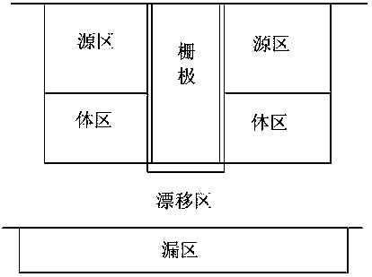
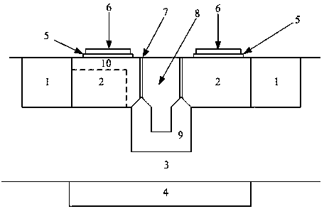
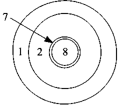
[0022] A vertical DMOS chip according to the present invention includes a vertical DMOS device, and the vertical DMOS device includes an A-type drain region 4, a B-type drift region 3 located above the A-type drain region, and a vertical gate 8 in the drift region. , the sidewall and bottom of the vertical gate are surrounded by a vertical gate insulating layer; a B-type body region 2 is provided outside the vertical gate insulating layer, and the B-type body region is arranged on the side away from the vertical gate insulating layer There is an A-type source region, the depth of the B-type body region is shallower than that of the vertical gate, a lateral gate insulating layer is arranged above the body region, and a lateral gate is arranged above the lateral gate insulating layer; the drift region is doped with The impurity concent...


PUM


Abstract

The invention discloses a longitudinal DMOS chip, and the chip comprises a longitudinal DMOS device. The longitudinal DMOS device comprises an A-type drain region, and a B-type drift region above the A-type drain region. The interior of the B-type drift region is provided with a longitudinal grid electrode, and a side wall and bottom of the longitudinal grid electrode are wrapped by a longitudinal grid electrode insulating layer. An outer side of the longitudinal grid electrode insulating layer is provided with a B-type body region, and a side, far from the longitudinal grid electrode insulating layer, of the B-type body region is provided with an A-type source region. The depth of the B-type body region is less than the depth of the longitudinal grid electrode. A lateral grid electrode insulating layer is located above the B-type body region, and a lateral grid electrode is disposed above the lateral grid electrode insulating layer. The doping density of the B-type drift region is lower than the doping density of the B-type body region. A type and B type are conductive types that carriers are hollow or electrons. The device remarkably improves the voltage endurance capability between source electrodes, and improves the current capability during conduction. A conductive trench comprises a lateral conduction direction and a longitudinal conduction direction, thereby improving the conduction breakdown voltage of the device.

Description

technical field [0001] The invention belongs to the field of semiconductor devices, and relates to a vertical DMOS chip. Background technique [0002] Similar in structure to CMOS devices, DMOS is composed of source, drain, gate, and body regions. DMOS also includes a drift region with lower doping concentration, so that a higher breakdown voltage can be obtained at the drain terminal. [0003] There are two main types of DMOS, vertical double-diffused metal oxide semiconductor field effect transistor VDMOS (vertical double-diffused MOSFET) and lateral double-diffused metal oxide semiconductor field effect transistor LDMOS (lateral double-dif fused MOSFET). Among them, VDMOS can obtain larger current conduction capability and lower on-resistance due to the vertical structure. At the same time, due to the existence of the drift region, the breakdown voltage value between the source and the drain is also higher. [0004] DMOS devices are composed of hundreds or thousands of s...

Claims


Application Information

Patent Timeline
Patent Type & Authority Applications(China)
IPC IPC(8): H01L29/78H01L29/08H01L29/423
CPCH01L29/7813H01L29/0865H01L29/4236H01L29/7831
Inventor 崔永明张干王建全王作义彭彪
Owner 四川广义微电子股份有限公司
Learn More