
NLDMOS device and manufacture method thereof

A manufacturing method and device technology, which is applied in semiconductor/solid-state device manufacturing, semiconductor devices, electrical components, etc., can solve the problem that the breakdown voltage is not easy to increase, and achieve the effect of increasing the conduction breakdown voltage

Inactive Publication Date: 2015-01-28
SHANGHAI HUAHONG GRACE SEMICON MFG CORP
View PDF5 Cites 1 Cited by
  • Summary
  • Abstract
  • Description
  • Claims
  • Application Information

AI Technical Summary

Problems solved by technology

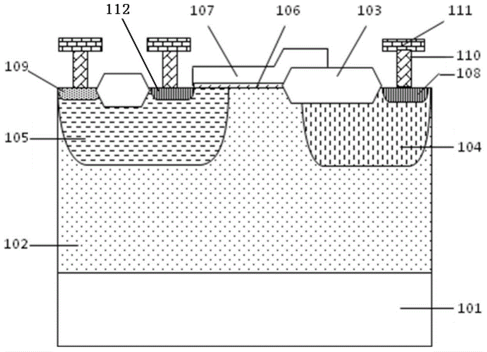
[0004] figure 1 In the NLDMOS device shown, the N-type deep well 102 and N-well 104 are sometimes shared with other devices, and the doping concentration cannot be changed, while the N-type deep well 102 is thicker and deeper, so it is not easy to be depleted, and the breakdown voltage is not easy to increase , the breakdown voltage of the device can only be improved by changing the device size and structure

Method used


Image

  • NLDMOS device and manufacture method thereof
  • NLDMOS device and manufacture method thereof
  • NLDMOS device and manufacture method thereof

Examples


Embodiment 1

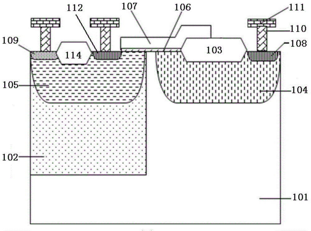
[0040] NLDMOS (N-type laterally diffused metal oxide semiconductor) devices, such as figure 2 As shown, an N-type deep well 102 is formed on the left part of the P-type silicon substrate 101;

[0041] A P well 105 is formed on the N-type deep well 102;

[0042] An N well 104 is formed on the right part of the P-type silicon substrate 101;

[0043] There is a P-type silicon substrate 101 spacer between the N-type deep well 102 and the N-well 104;

[0044] The P well 105 has a channel region field oxygen 114 formed in the middle;

[0045] A heavily doped P-type region 109 is formed on the P well 105 on the left side of the field oxygen 114 in the channel region, and a heavily doped N-type region 112 is formed on the P well 105 on the right side of the field oxygen in the channel region;

[0046] A drift region field oxygen 103 is formed in the middle of the N well 104; a heavily doped N-type region 108 is formed on the N well 104 on the right side of the drift region field o...

Embodiment 2

[0057] The manufacturing method of the NLDMOS device of Embodiment 1 mainly includes the following process steps:

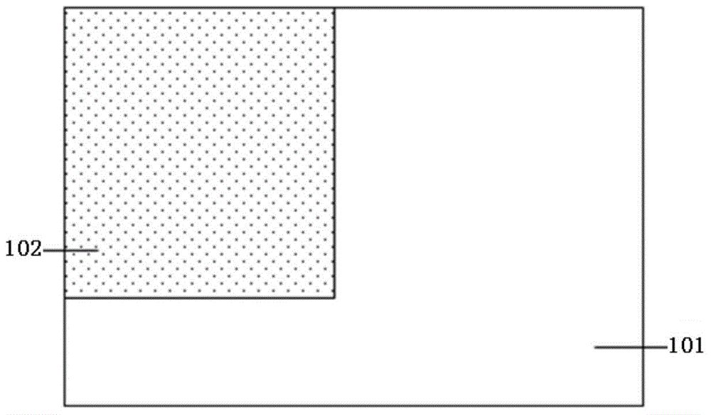
[0058] 1. On the left part of the P-type substrate 101, an N-type deep well 102 is formed by N-type ion implantation, such as image 3 shown;

[0059] 2. Utilize photolithography in the active region to open the field oxygen region, etch the field oxygen region, grow the field oxygen, form the field oxygen 114 in the channel region on the N-type deep well 102, and form the drift on the right part of the P-type substrate 101 Field Oxygen 103, such as Figure 4 shown;

[0060] 3. Photolithography opens the well implantation area, implants P-type impurity ions into the N-type deep well 102 below the channel region field oxygen 114 and its left and right sides to form a P well 105, and forms a P well 105 under the field oxygen 103 in the drift region and its left and right sides. N well 104 is formed by implanting N-type impurity ions into the P-type substrate 101...


PUM


Abstract

The invention discloses an NLDMOS device. An N-type deep trap is formed at the left portion of a P-type silicon substrate; a P trap is formed in the N-type deep trap; an N trap is formed at the right portion of the P-type silicon substrate; and a P-type silicon substrate interval zone is arranged between the N-type deep trap and the N trap. The invention also discloses a manufacture method of the NLDMOS device. According to the NLDMOS device and the manufacture method thereof, the deep N trap wraps the P trap so as to enable the P trap to be isolated from the substrate; the dimension of the N-type deep trap is reduced to the P trap which is taken as the channel zone of an NLDMOS, it is ensured that the P trap is isolated from the substrate, and the N-type deep trap is not formed at the N trap which is taken as the drifting zone of the NLDMOS, such that the N-type doping concentration in the drifting zone is decreased, and accordingly, the off-BV of the device is increased; and the dimension of the N trap is increased to the portion between the N-type deep trap and a beak, and the N-type doping concentration below a gate oxide layer is increased, such that the on-BV is increased, and at the same time, it is ensured that the on-resistance is not too large.

Description

technical field [0001] The invention relates to semiconductor technology, in particular to an NLDMOS device and a manufacturing method thereof. Background technique [0002] LDMOS (Laterally Diffused Metal Oxide Semiconductor) is currently widely used in power management circuits due to its advantages of high voltage resistance, high current drive capability, extremely low power consumption, and integration with CMOS. [0003] There is a 40V isolated NLDMOS (N-type laterally diffused metal oxide semiconductor) device, such as figure 1 As shown, an N-type deep well 102 is formed on a P-type silicon substrate 101, a P well 105 is formed on the left of the N-type deep well 102, and an N well 104 is formed on the right; between the P well 105 and the N well 104, there is N-type deep well 102 spacer, P well 105 right, N well 104 left and P well 105 and N well 104 are formed above the N-type deep well 102 spacer; polysilicon gate 107 is the same as P well The right part of 105, ...

Claims


Application Information

Patent Timeline
IPC IPC(8): H01L29/78H01L29/06H01L21/336
CPCH01L29/7816H01L29/0611H01L29/66681
Inventor 段文婷刘冬华钱文生
Owner SHANGHAI HUAHONG GRACE SEMICON MFG CORP
Learn More