Method for forming planar thick isolation medium
A technology of isolating media and planarization, applied in the direction of electrical components, semiconductor/solid-state device manufacturing, circuits, etc., can solve the problems of microwave signal loss, current capacity limitation, limiting device performance and process yield, etc., to ensure flatness, Effect of Reducing Parasitic Capacitance
- Summary
- Abstract
- Description
- Claims
- Application Information
AI Technical Summary
Problems solved by technology
Method used
Image


Examples
Embodiment 1
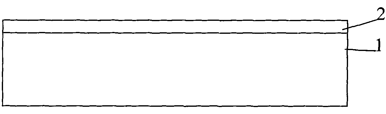
[0039] 1) Select an arsenic-doped silicon substrate region with a thickness of 560 μm and a resistivity of ≤0.003Ω·cm, and its silicon epitaxial layer is doped with phosphorus (n-type), with a resistivity of 0.5Ω·cm and a thickness of 1 μm (attached image 3 );
[0040] 2) Oxidative growth of 0.06 μm silicon dioxide under dry oxygen conditions at 920°C (attached Figure 4 );
[0041] 3), using LPCVD process to deposit a layer of silicon nitride with a thickness of 0.1 μm on the surface of the silicon substrate; (attached Figure 5 );
[0042] 4) Coat a layer of photoresist on the surface of the silicon substrate with a thickness of 1.0 μm, and form an array of etching windows with a spacing of 1.0 μm and 1.2 μm by photolithography, and use a reactive ion etching process to etch away the silicon nitride and silicon nitride in the windows. Silicon dioxide; use ICP to etch the silicon in the process window to form a 1.0 μm deep hole, and finally remove the photoresist (attache...
Embodiment 2
[0048] 1) Select an arsenic-doped silicon substrate region with a thickness of 420 μm and a resistivity of ≤0.003Ω·cm, and its silicon epitaxial layer is doped with phosphorus (n-type), with a resistivity of 500Ω·cm and a thickness of 100 μm (attached image 3 );
[0049] 2) Oxidative growth of 0.08 μm silicon dioxide under dry oxygen conditions at 960°C (attached Figure 4 );
[0050] 3), using LPCVD process to deposit a layer of silicon nitride with a thickness of 0.2 μm on the surface of the silicon substrate; (attached Figure 5 );
[0051] 4) Apply a layer of photoresist on the surface of the silicon substrate with a thickness of 1.5 μm, and form an array of etching windows with a spacing of 1.5 μm and 1.4 μm by photolithography, and use a reactive ion etching process to etch away the silicon nitride and silicon nitride in the windows. Silicon dioxide; use ICP to etch the silicon in the process window to form a 100 μm deep hole, and finally remove the photoresist (atta...
Embodiment 3
[0057] 1) Select an arsenic-doped silicon substrate region with a thickness of 380 μm and a resistivity of ≤0.003Ω·cm, and its silicon epitaxial layer is doped with phosphorus (n-type), with a resistivity of 1000Ω·cm and a thickness of 200 μm (attached image 3 );
[0058] 2) Oxidative growth of 0.1 μm silicon dioxide under dry oxygen conditions at 1000°C (attached Figure 4 );
[0059] 3), utilize the LPCVD process to deposit a layer of silicon nitride with a thickness of 0.3 μm on the surface of the silicon substrate; (attached Figure 5 );
[0060] 4) Coat a layer of photoresist on the surface of the silicon substrate with a thickness of 2.5 μm, and form an array of etched windows with a pitch of 2.0 μm and 1.8 μm by photolithography, and use a reactive ion etching process to etch away the silicon nitride and silicon nitride in the windows. Silicon dioxide; use ICP to etch the silicon in the process window to form a 200 μm deep hole, and finally remove the photoresist (a...
PUM
 Abstract
Description
Claims
Application Information
 - Generate Ideas
- Intellectual Property
- Life Sciences
- Materials
- Tech Scout
- Unparalleled Data Quality
- Higher Quality Content
- 60% Fewer Hallucinations
Browse by: Latest US Patents, China's latest patents, Technical Efficacy Thesaurus, Application Domain, Technology Topic, Popular Technical Reports.
© 2025 PatSnap. All rights reserved.Legal|Privacy policy|Modern Slavery Act Transparency Statement|Sitemap|About US| Contact US: help@patsnap.com