Surface-enhanced Raman scattering underlay of #-shaped nano electromagnetic super medium
A technology of surface-enhanced Raman and electromagnetic metamedia, which is applied in the field of surface spectroscopy, can solve the problems that restrict the reliability of quantitative analysis of surface-enhanced Raman scattering technology and the practical industrial application, particle size, shape distribution state and agglomeration state are difficult to control, Instability of experimental results and other problems, to achieve high stability, improve reproducibility, neatly arranged effect
- Summary
- Abstract
- Description
- Claims
- Application Information
AI Technical Summary
Problems solved by technology
Method used
Image
Examples
Embodiment 1
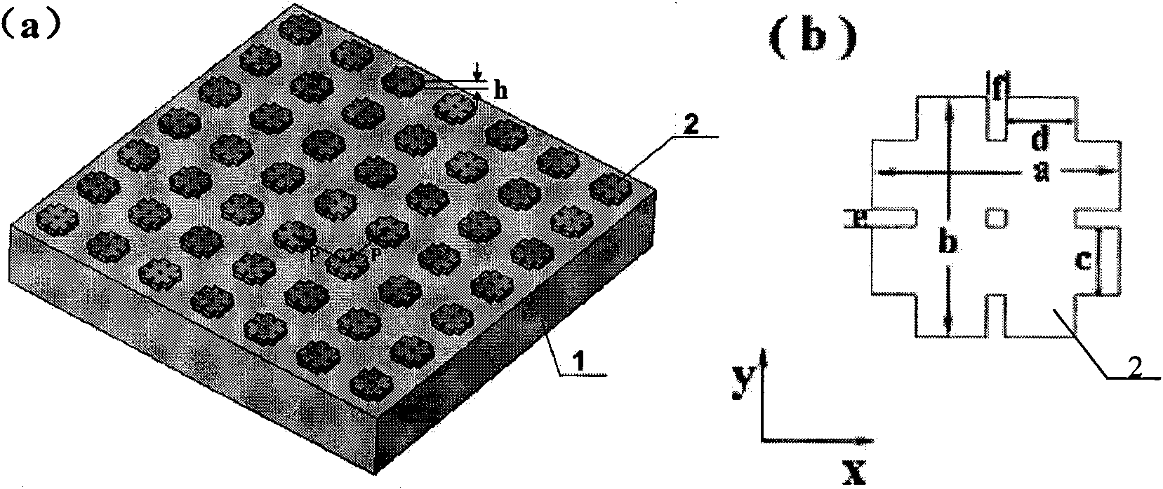
[0029] Such as figure 1 As shown in a and b, refer to the nanoimprint lithography disclosed in the document Kebin Li et al.Surface enhanced Raman scattering on long-rangd ordered noble-metal nanocrescent arrays, Nanotechnology 19 (2008) 145305, using metal material gold on the substrate glass 1 constructs a #-shaped nanostructure unit 2, two horizontal bars or two vertical bars are parallel to each other, and the horizontal bars and vertical bars are perpendicular to each other. At the same time, the nanostructure unit 2 is periodically on the two axes of the substrate glass 1 ( P=260nm) are arranged to form a two-dimensional array structure, wherein the length of the horizontal or vertical rods a=b=140nm, the width of the horizontal or vertical rods c=d=40nm, the distance between the horizontal or vertical rods e=f=10nm, and the horizontal or vertical rods Or vertical bar thickness h=30nm.
[0030] Effect example
[0031]In the following effect example, the three-dimensiona...
Embodiment 2
[0034] Using #-shaped gold nano-electromagnetic metamedia as a surface-enhanced Raman scattering substrate:
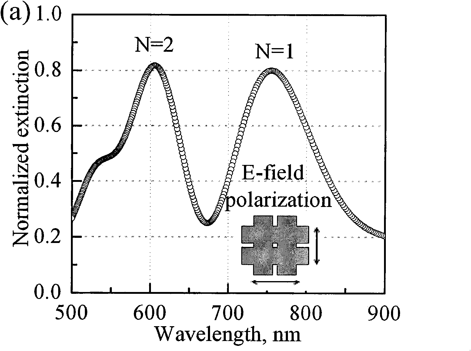
[0035] Such as figure 1 As shown, gold is used as the metal material to construct the #-shaped nano-electromagnetic supermedium on the glass substrate, the length of the nanorod a=b=140nm, the width c=d=40nm, the thickness h=30nm, the spacing e=f=10nm, the structure The cell period P=260nm. The resulting extinction spectrum is as figure 2 As shown, there are two strong plasmon resonance peaks at 753nm and 605nm respectively, accompanied by a weaker third-order mode at about 529nm. Due to the symmetry of the structure, the same dual-band response effect can be obtained when the incident light is polarized along the x or y direction.
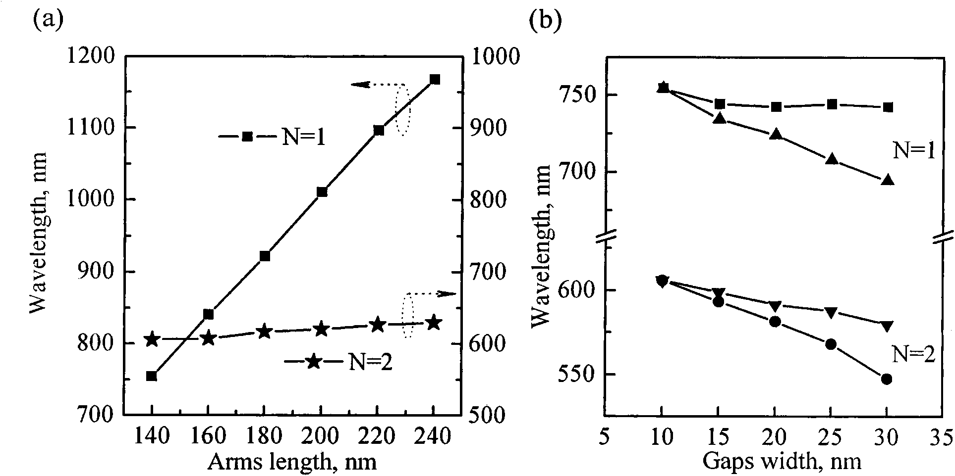
[0036] The resonance wavelength of this structure can be adjusted in a large range (547-1168nm). When the polarization direction of the incident light is along the vertical rod (ie, the y direction), the rod length a is increased from ...
Embodiment 3
[0039] The #-shaped silver nano-electromagnetic metamedia is used as the surface-enhanced Raman scattering substrate.
[0040] Such as figure 1 As shown, silver is used as the metal material to construct the #-shaped nano-electromagnetic supermedium on the silicon substrate, the length of the nanorod a=b=140nm, the width c=d=40nm, the thickness h=30nm, the spacing e=f=10nm, the unit Period P = 260nm. The resulting extinction spectrum is as Figure 5 As shown, there are two strong plasmon resonance peaks located at 664nm and 503nm respectively. Due to the symmetry of the structure, the same dual-band response effect can be obtained when the incident light is polarized along the x or y direction.
[0041] The resonance wavelength of this structure can be adjusted in a large range (477-1074nm). When the polarization direction of the incident light is along the vertical rod (ie, the y direction), the rod length a is increased from 140nm to 240nm, and N=1 The central wavelength...
PUM
 Abstract
Description
Claims
Application Information
 - R&D
- Intellectual Property
- Life Sciences
- Materials
- Tech Scout
- Unparalleled Data Quality
- Higher Quality Content
- 60% Fewer Hallucinations
Browse by: Latest US Patents, China's latest patents, Technical Efficacy Thesaurus, Application Domain, Technology Topic, Popular Technical Reports.
© 2025 PatSnap. All rights reserved.Legal|Privacy policy|Modern Slavery Act Transparency Statement|Sitemap|About US| Contact US: help@patsnap.com


