
Graded zinc diffusing method based on MOCVD (Metal-Organic Chemical Vapor Deposition) system for producing chip of indium-gallium-arsenic photoelectric detector

A technology of photodetector and diffusion method, applied in circuits, electrical components, semiconductor devices, etc., can solve the problems of low P-InP carrier concentration, complex process, low doping impurities, etc. Production, process repeatability, precise control effect

Active Publication Date: 2009-10-28
WUHAN HUAGONG GENUINE OPTICS TECH
View PDF0 Cites 11 Cited by
  • Summary
  • Abstract
  • Description
  • Claims
  • Application Information

AI Technical Summary

Problems solved by technology

The InP / InGaAs PIN detector epitaxial material is mainly prepared by MOCVD, and the epitaxial structure does not contain high-concentration P-type doping. The P-type InP or InGaAs ohmic contact layer required for device production is completed by various forms of Zn diffusion. Zn The traditional methods of diffusion include the closed tube diffusion method and the open tube diffusion method. The sample is in a closed or open quartz boat, and ZnAs and ZnP saturated vapor are used as the diffusion source. The advantage of the two methods is that the diffusion equipment is simple, but there are the following problems: Because ZnAs and ZnP are not stable enough, the doping of P-InP is relatively low, about 1.8E+17 / cm3; the interface formed by InP and InGaAs is not clear enough, and it is easy to accumulate too much at the junction of InP and InGaAs interface. Too many charge particles, too much charge accumulation will also cause the absorption of redundant impurity particles, resulting in excessive dark current; the process is complicated and the process controllability is poor; the P-InP carrier concentration is too low, it is difficult to achieve good The ohmic contact of , is greatly restricted for making high linear devices.

Method used

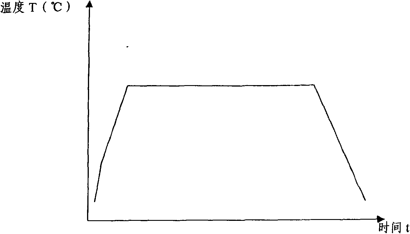
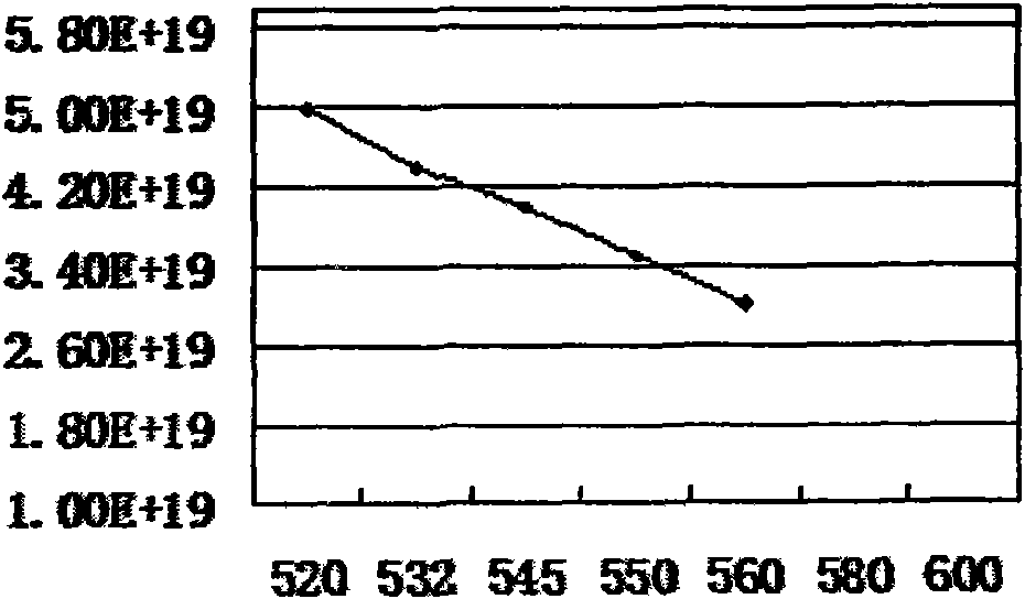
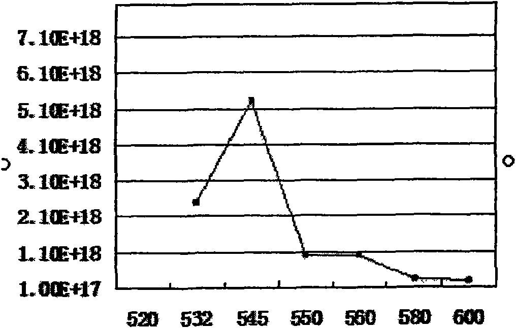

Image

  • Graded zinc diffusing method based on MOCVD (Metal-Organic Chemical Vapor Deposition) system for producing chip of indium-gallium-arsenic photoelectric detector
  • Graded zinc diffusing method based on MOCVD (Metal-Organic Chemical Vapor Deposition) system for producing chip of indium-gallium-arsenic photoelectric detector
  • Graded zinc diffusing method based on MOCVD (Metal-Organic Chemical Vapor Deposition) system for producing chip of indium-gallium-arsenic photoelectric detector

Examples


Embodiment Construction

[0025] The applicant found the following points in the research:

[0026] 1. There is a big difference in the diffusion law of zinc in InP and InGaAs materials. It is easy to diffuse in InP materials, but the diffusion rate of zinc in InGaAs materials is slow.

[0027] 2. There is a certain limit to the diffusion depth. For detectors with InGaAs PIN structure, the InGaAs layer needs to have a higher carrier concentration, but the zinc at this flow rate has oversaturated the InP layer, which will cause adverse effects, and between InP and InGaAs The interface formed by the material is not clear enough, and it is easy to accumulate too many charged particles at the junction of the InP and InGaAs interface.

[0028] In order to make both InP and InGaAs materials obtain higher carrier concentrations and clear PN junction interfaces, the applicant accurately calculated the diffusion time of each layer of materials, and when the InP layer with a certain thickness is diffused and ent...


PUM


Abstract

The invention relates to a graded zinc diffusing method based on an MOCVD system for producing the chip of an indium-gallium-arsenic photoelectric detector. The method comprises the following steps: a semiconductor wafer which does not form an InGaAs PIN structure of a PN junction is cleaned and blown to dry by high-purity nitrogen; an MOCVD reaction chamber is heated up, depressurized and cleaned; the semiconductor wafer is placed in the reaction chamber; the pressure of the reaction chamber is set; diffusion taking a zinc phosphide compound which is formed by zinc methide (DMZn) and phosphorane (PH3) at high temperature as a diffusion source is conducted with the presence of catalytic reaction and the shielding gas; after the completion of the diffusion, the gas is turned off, the reaction chamber is cooled down and filled with nitrogen and has a pressure rise; and the wafer which undergoes the diffusion is taken out of the reaction chamber. As the diffusion rules of zinc in InP material and InGaAs material have great difference, the graded diffusion method is adopted. With the method, both the InP layer and the InGaAs layer can have rather high current carrier concentration, good interface, rather good homogeneity, technique repeatability, high response and precise control and can be manufactured on a large scale.

Description

technical field [0001] The invention relates to a gradual zinc diffusion method for making an indium gallium arsenic photodetector chip based on an MOCVD system. Background technique [0002] InP-based InGaAs PIN photodetectors are widely used in the field of optical fiber communication. As the core component of light receiving in communication, CATV system, and optoelectronic technology, its application space is very huge. The InP / InGaAs PIN detector epitaxial material is mainly prepared by MOCVD, and the epitaxial structure does not contain high-concentration P-type doping. The P-type InP or InGaAs ohmic contact layer required for device production is completed by various forms of Zn diffusion. Zn The traditional methods of diffusion include the closed tube diffusion method and the open tube diffusion method. The sample is in a closed or open quartz boat, and ZnAs and ZnP saturated vapor are used as the diffusion source. The advantage of the two methods is that the diffusi...

Claims


Application Information

Patent Timeline
Patent Type & Authority Applications(China)
IPC IPC(8): H01L31/18C23C16/44
CPCY02P70/50
Inventor 吴瑞华刘建军
Owner WUHAN HUAGONG GENUINE OPTICS TECH
Learn More