Preparation method for complementary metal oxide semiconductor element with dual metal grid

An oxide semiconductor and double metal gate technology, which is applied in the field of complementary metal oxide semiconductor components, can solve the problems of complex integration technology and process control, and strict requirements for material thickness and composition control.

Active Publication Date: 2012-09-19
UNITED MICROELECTRONICS CORP
View PDF0 Cites 0 Cited by
  • Summary
  • Abstract
  • Description
  • Claims
  • Application Information

AI Technical Summary

Problems solved by technology

[0004] Dual-function metal gates are either paired with NMOS elements or PMOS elements, which makes the integration technology and process control of related elements more complicated, and the thickness and composition control requirements of each material are also more stringent.

Method used


Image

  • Preparation method for complementary metal oxide semiconductor element with dual metal grid
  • Preparation method for complementary metal oxide semiconductor element with dual metal grid
  • Preparation method for complementary metal oxide semiconductor element with dual metal grid

Examples


Embodiment Construction

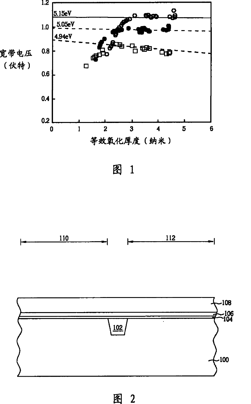
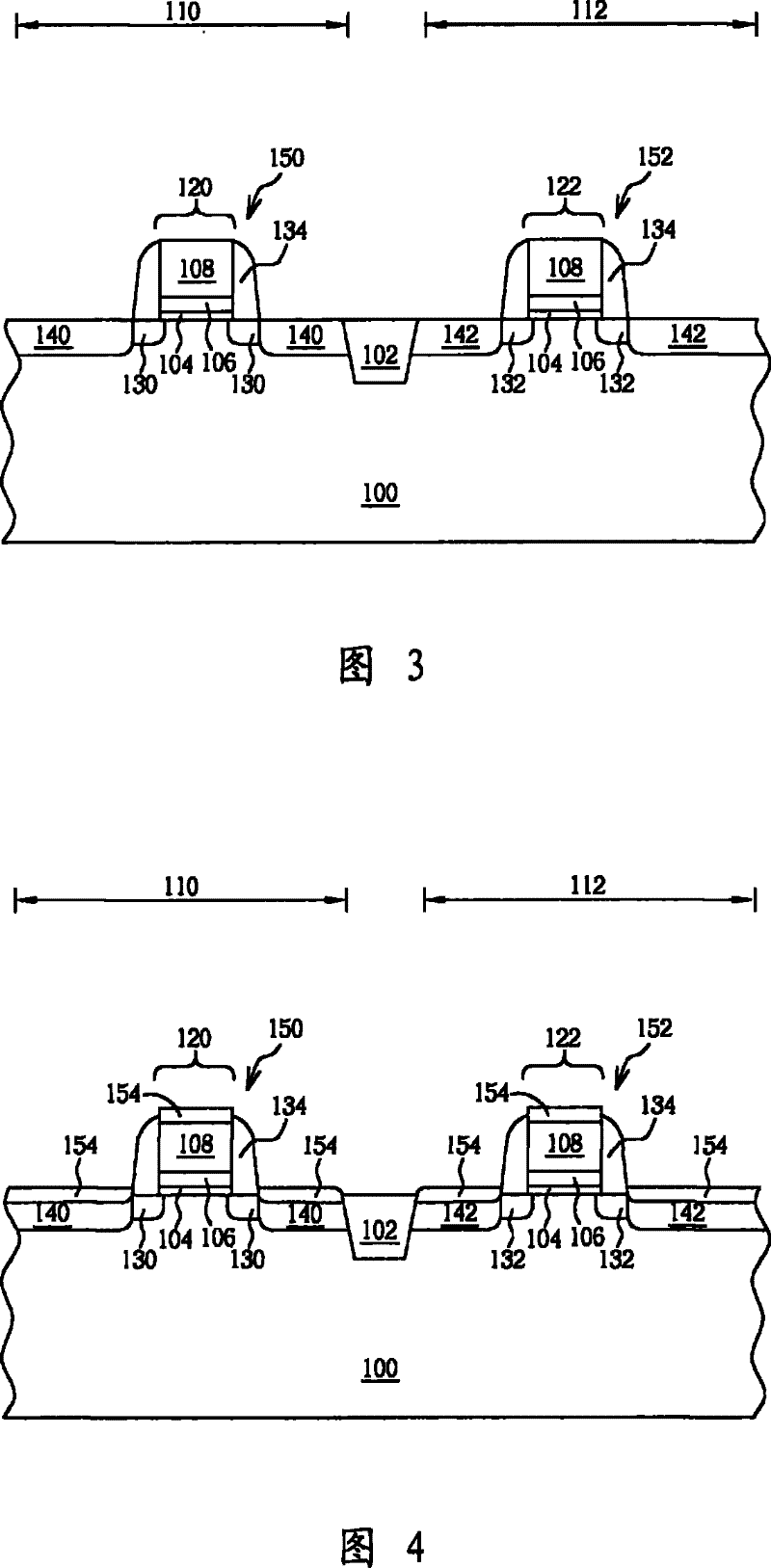
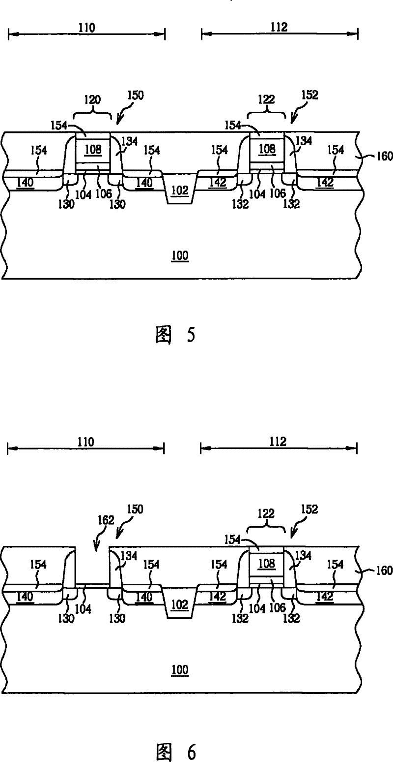
[0041] see Figure 2 to Figure 8 , Figure 2 to Figure 8 It is a schematic diagram of the first preferred embodiment of the method for manufacturing a CMOS device with a double metal gate provided by the present invention. Such as figure 2As shown, a substrate 100 is firstly provided, such as a silicon substrate, a silicon-containing substrate, or a silicon-on-insulator (hereinafter referred to as SOI) substrate, etc., and a first active region 110 and a second active region 110 are defined on the surface of the substrate 100. The active region 112 , and a shallow trench isolation (STI) 102 for electrically isolating the first active region 110 and the second active region 112 is formed in the substrate 100 . Next, a high dielectric constant (hereinafter referred to as High-K) gate dielectric layer 104 , a tantalum carbide (TaC) layer 106 , and a polysilicon layer 108 are sequentially formed on the substrate 100 . In addition, in the first embodiment, a protection layer (n...


PUM


Abstract

The invention discloses a production method of a CMOS element with bimetal grids. The method comprises: a first conductive transistor and a second conductive transistor are formed respectively on a substrate that is provided with a first active area, a second active area and a shallow trench isolation providing an electric isolation; a metal silicide technology is carried out; an internal dielectric layer is formed on the substrate; a first etching technology is carried out; a part of grid of the first conductive transistor is removed and an opening is formed; and a high-dielectric constant gird dielectric layer of the first conductive transistor is exposed on the bottom of the opening, and a first metal layer is formed in the opening.

Description

technical field [0001] The present invention relates to a manufacturing method of a complementary metal-oxide semiconductor (hereinafter referred to as CMOS) element with a dual metal gate, especially a gate last ) process with a double metal gate CMOS element manufacturing method. Background technique [0002] As the size of CMOS devices continues to shrink, the traditional method of reducing the gate dielectric layer, such as reducing the thickness of the silicon dioxide layer, to achieve the purpose of optimization, is facing problems caused by the tunneling effect of electrons. Physical limitation of excessive leakage current. In order to effectively extend the generation evolution of logic elements, high dielectric constant (hereinafter referred to as High-K) materials can effectively reduce the physical limit thickness, and at the same equivalent oxide thickness (equivalent oxide thickness, hereinafter referred to as EOT) Under the advantages of effectively reducing ...

Claims


Application Information

Patent Timeline
Patent Type & Authority Patents(China)
IPC IPC(8): H01L21/8238H01L21/28
Inventor 林建廷程立伟许哲华马光华杨进盛
Owner UNITED MICROELECTRONICS CORP
Why Eureka
Try Eureka