PV film layer for improving electrode ring adhesion and adhesion improvement method
An adhesion and electrode ring technology, applied in circuits, electrical components, semiconductor devices, etc., can solve problems such as falling off, and achieve the effect of protecting electrodes, improving the problem of falling rings, and good insulation.
- Summary
- Abstract
- Description
- Claims
- Application Information
AI Technical Summary
Problems solved by technology
Method used
Image
Examples
Embodiment Construction
[0022] The embodiments of the present invention will be described in detail below with reference to the accompanying drawings, but the present invention can be implemented in various ways defined and covered by the claims.
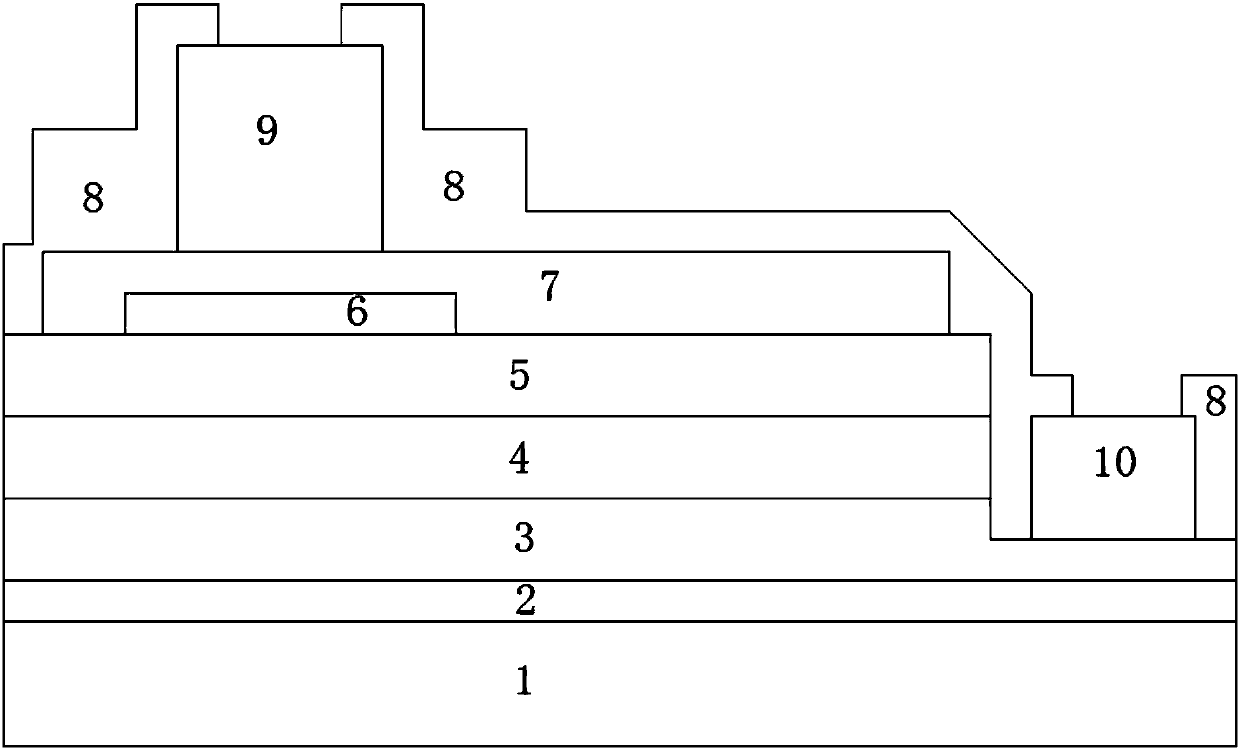
[0023] see figure 1 , the structure of the epitaxial wafer can be found in figure 1 , including substrate material 1, buffer layer 2, N-type semiconductor layer (N-GaN layer) 3, multiple quantum well layer (MQW) 4, P-type semiconductor layer (P-GaN layer) 5, current blocking layer from bottom to top layer (CB layer) 6 , current spreading layer (ITO layer) 7 , transparent insulating layer (PV layer) 8 , and P electrode 9 and N electrode 10 . Wherein, the transparent insulating layer (PV layer) 8 is a SiNO thin film layer.
[0024] The preparation process is as follows:
[0025] The epitaxial wafer prepared with the CB pattern is evaporated with a layer of transparent conductive layer ITO material as the current spreading layer by evaporation method. The...
PUM
 Abstract
Description
Claims
Application Information
 - Generate Ideas
- Intellectual Property
- Life Sciences
- Materials
- Tech Scout
- Unparalleled Data Quality
- Higher Quality Content
- 60% Fewer Hallucinations
Browse by: Latest US Patents, China's latest patents, Technical Efficacy Thesaurus, Application Domain, Technology Topic, Popular Technical Reports.
© 2025 PatSnap. All rights reserved.Legal|Privacy policy|Modern Slavery Act Transparency Statement|Sitemap|About US| Contact US: help@patsnap.com


