
Copper-clad laminate, printed wiring board, multilayer printed wiring board, and methods for producing those

A printed circuit board, multi-layer printing technology, applied in the direction of printed circuit manufacturing, multilayer circuit manufacturing, printed circuit, etc., can solve the problem of unavoidable high-frequency signal energy loss, waveform disorder, inability to give full play to the excellent characteristics of fluororesin, signal The problems of increased transmission time and current loss can achieve the effect of easy fine patterning, excellent ductility and toughness, and reduced conductor loss.

Active Publication Date: 2008-10-01
NIPPON PILLAR PACKING CO LTD +1
View PDF1 Cites 21 Cited by
  • Summary
  • Abstract
  • Description
  • Claims
  • Application Information

AI Technical Summary

Problems solved by technology

As a result, not only the current loss becomes larger, but when the skin depth is smaller than the surface thickness of the conductor, the current flows through the uneven surface of the conductor, the transmission distance becomes longer, and the time required for signal transmission and current loss become larger
[0009] In this way, the actual situation of the conventional fluororesin copper foil laminates is that in order to ensure the bonding strength, the surface of the copper foil has to be roughened or blackened. Therefore, the energy loss and waveform disturbance of the high-frequency signal cannot be avoided. Give full play to the unique excellent characteristics of fluororesin (low dielectric constant characteristics in high frequency band, low dielectric loss tangent characteristics)
In addition, multilayer printed wiring boards are formed with IVH (internal via hole) and / or BVH (blind via hole) in order to achieve high circuit density, but when PFA film is used as the adhesive resin film, the molding temperature needs to be 380 °C or higher (for example, refer to paragraph 0026 of Patent Document 1), therefore, IVH and BVH may be crushed when thermoforming a printed wiring board laminate, making it difficult to obtain a multilayer printed wiring board with IVH and BVH

Method used


Image

  • Copper-clad laminate, printed wiring board, multilayer printed wiring board, and methods for producing those
  • Copper-clad laminate, printed wiring board, multilayer printed wiring board, and methods for producing those
  • Copper-clad laminate, printed wiring board, multilayer printed wiring board, and methods for producing those

Examples


Embodiment

[0045] As an example, the following copper foil laminated boards No. 1 and No. 2 were produced.

[0046] That is, first, alternately repeat the process at a weight per unit area of ​​24g / m 2 The process of impregnating the PTFE dispersant with a concentration of 60% in the E glass cloth, and the process of drying the PTFE dispersant at a temperature of 305°C lower than the melting point of PTFE (327°C) to obtain PTFE A first prepreg having a resin impregnation rate of 91.5% and a thickness of 130 μm. In addition, a total of five first prepregs were produced including the four first prepregs used in the comparative example described later.

[0047] In addition, it is repeated alternately when the weight per unit area is 12g / m 2 The process of impregnating the PTFE dispersant with a concentration of 60% in the E glass cloth, and the process of drying the PTFE dispersant at a temperature of 305°C lower than the melting point of PTFE (327°C) to obtain PTFE The second prepreg ha...


PUM

PropertyMeasurementUnit
thicknessaaaaaaaaaa
thicknessaaaaaaaaaa
surface roughnessaaaaaaaaaa

Abstract

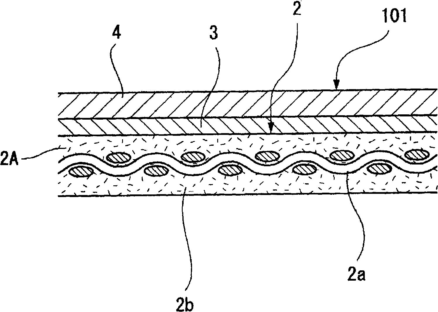
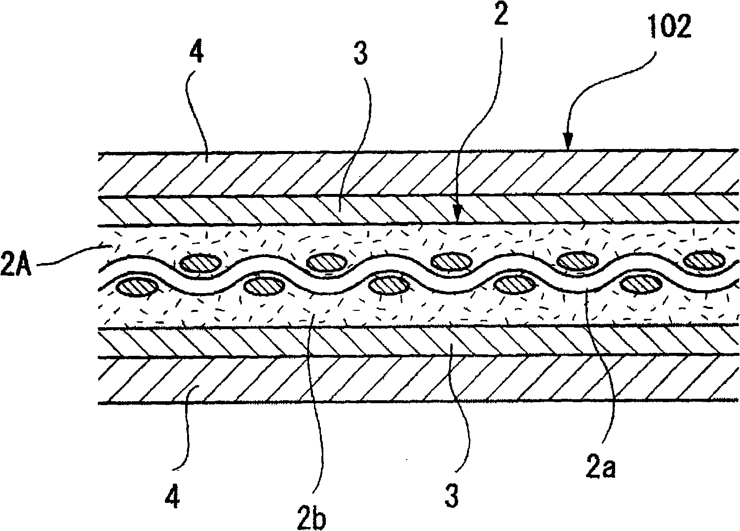
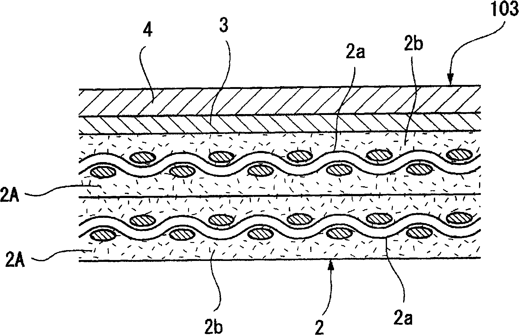
Disclosed is a copper-clad laminate wherein the copper foil adhesion strength (copper foil peeling strength) is greatly improved without subjecting the copper foil surface to a roughening treatment or a blackening treatment, a printed-wiring board, a multi-layer printed-wiring board and manufacturing method thereof. This copper-clad laminate can be adequately used in a high frequency region. Specifically disclosed is a copper-clad laminate (101) for single-sided printed wiring boards, which is obtained by bonding a copper foil (4) onto one surface of an insulating substrate (2), which is composed of a fluoroplastic prepreg (2A), via a composite film (3) of LCP and PFA. The copper foil (4) is a rolled copper foil having a smooth surface without being subjected to a roughening treatment or a blackening treatment on both sides. The insulating substrate (2) and the copper foil (4) are bonded with each other via the composite film (3) by being fired and pressed at a temperature higher than the melting point of PFA by 5-40 DEG C and lower than the melting point of LCP.

Description

technical field [0001] The present invention relates to a copper foil laminate for printed wiring boards that can be used well in a high-frequency region, and a manufacturing method thereof, and to a printed wiring board and a multilayer printed wiring board composed of the copper foil laminate, and to their manufacture According to the method, the above-mentioned copper foil laminate is formed by bonding copper foil to an insulating substrate made of fluororesin through a resin film for bonding. Background technique [0002] Copper foil laminates made by bonding copper foil to insulating substrates made of fluororesin, printed wiring boards and multilayer printed wiring boards composed of the copper foil laminates, depending on the characteristics of the fluororesin used as the material for the dielectric layer, It is also suitable for use in high-frequency regions above GHz where the dielectric loss tangent (tan δ) is small. [0003] Moreover, it is well known that such a...

Claims


Application Information

Patent Timeline
Patent Type & Authority Applications(China)
IPC IPC(8): B32B15/082B32B15/09B32B15/08H05K3/46
CPCH05K2201/015H05K1/0366H05K2201/0141Y10T428/31544B32B15/08H05K1/036H05K1/034Y10T442/3415H05K3/386B32B5/024B32B7/12B32B15/14B32B15/20B32B2260/021B32B2260/046B32B2262/101B32B15/082B32B15/09H05K3/46
Inventor 岛内浩一伊藤博文李庭昌
Owner NIPPON PILLAR PACKING CO LTD
Learn More