Oxidate magnetic semiconductor thin film capable of regulating electric transport property and method of preparing the same

A magnetic semiconductor and electrical transport technology, applied in the field of information technology spintronic materials, can solve the problems of regulation, unknown electron transport properties, unclear reasons for the electrical transport properties of oxide magnetic semiconductor thin film materials, etc. The effect of high Curie temperature and large magnetism

Inactive Publication Date: 2008-09-03
SHANDONG UNIV
View PDF2 Cites 15 Cited by
  • Summary
  • Abstract
  • Description
  • Claims
  • Application Information

AI Technical Summary

Problems solved by technology

[0005] However, so far, the reasons that affect the electrical transport properties of oxide magnetic semiconductor thin film materials are not clear, let alone how to regulate the electronic transport properties

Method used


Image

  • Oxidate magnetic semiconductor thin film capable of regulating electric transport property and method of preparing the same
  • Oxidate magnetic semiconductor thin film capable of regulating electric transport property and method of preparing the same
  • Oxidate magnetic semiconductor thin film capable of regulating electric transport property and method of preparing the same

Examples


Embodiment 1

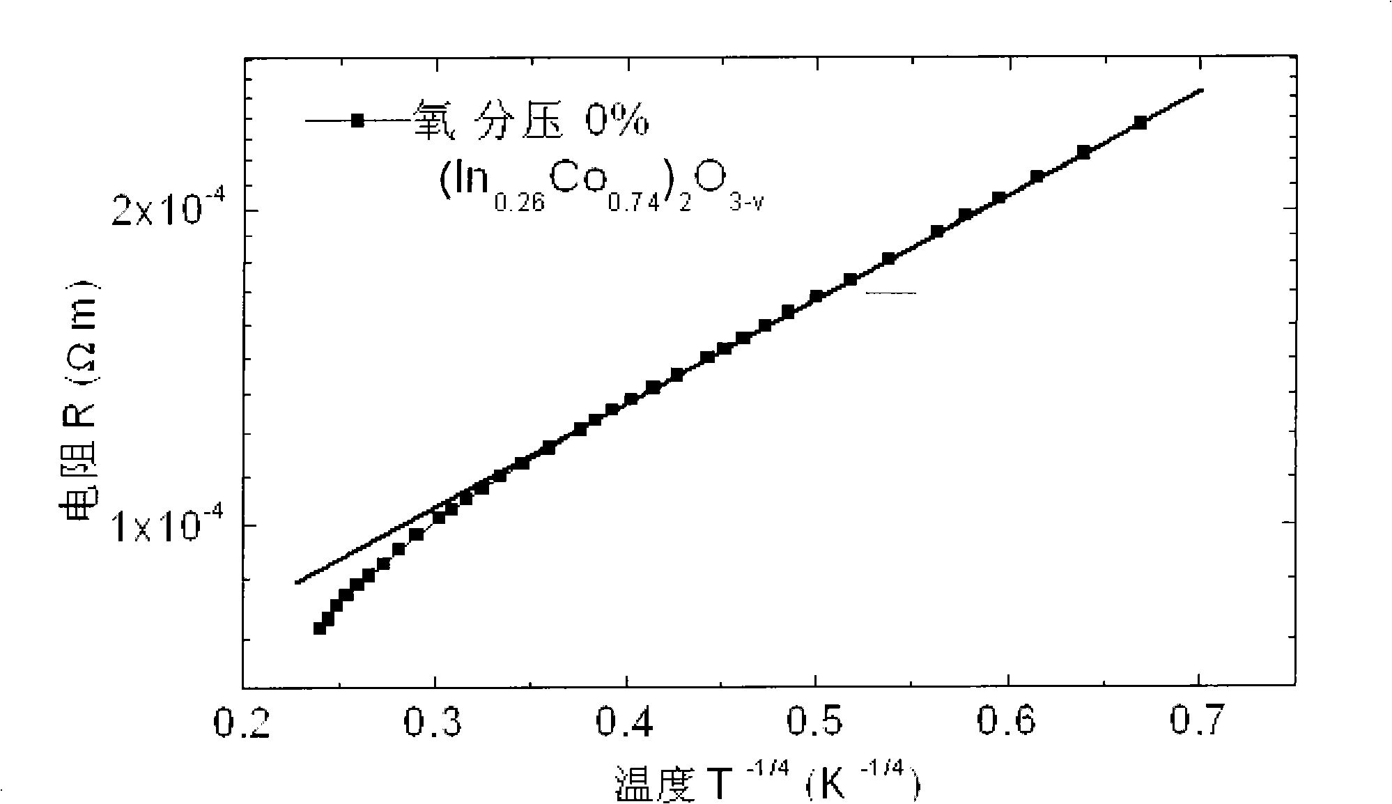
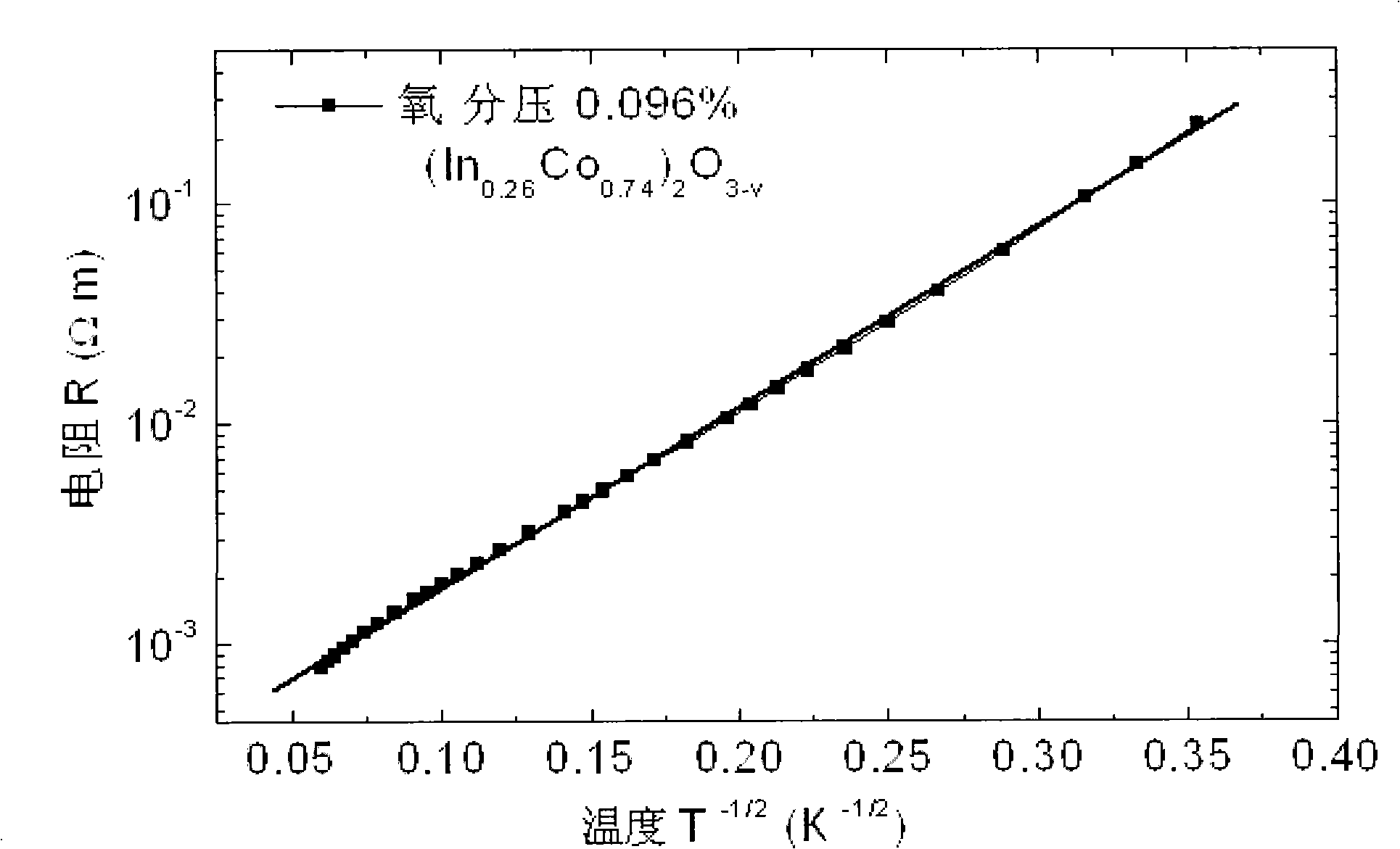
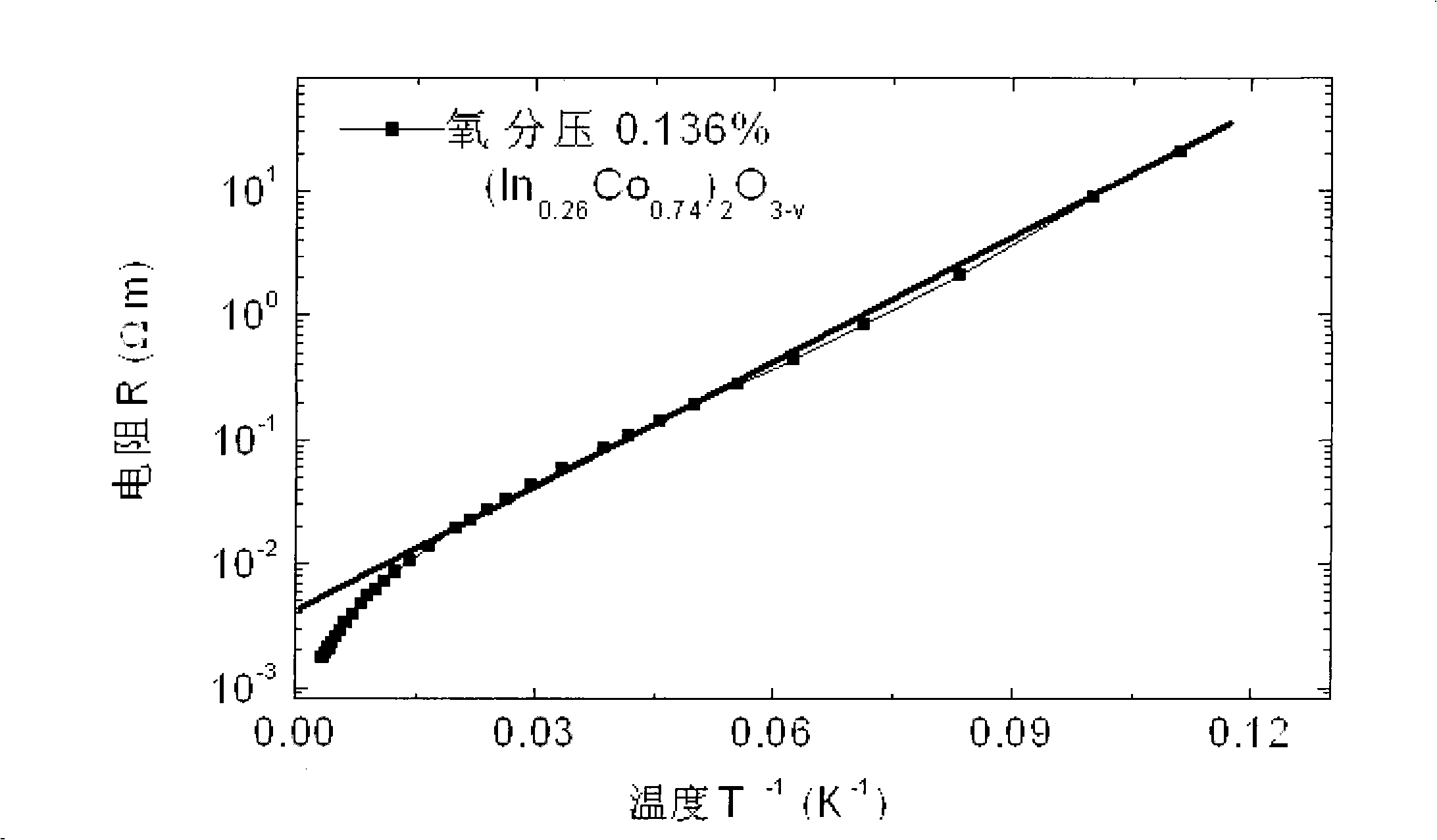
[0034] Embodiment 1: (In 0.26 co 0.74 ) 2 o 3-v The preparation of oxide magnetic semiconductor thin films and the control of their electrical transport properties use the method of magnetron sputtering, and the sputtering chamber is vacuumed to 5×10 -5 Pa, based on In with a purity of 99.99% or more 2 o 3 Ceramics and Co metal with a purity of more than 99.99% are used as targets, and In 2 o 3 Placed on the RF target, Co placed on the DC target. With high-purity Ar gas with a purity of more than 99.99% and O 2 The Ar gas with a molar ratio of 2% was used as the sputtering atmosphere, and the two gases were respectively entered into the gas mixing chamber through the gas mass flow meter, and after being thoroughly mixed uniformly in the gas mixing chamber, they entered the sputtering chamber. The pressure of the sputtering chamber was kept at 1Pa. The partial pressure of oxygen is controlled by a mass flow meter, and in this example, the partial pressures of oxygen ar...

Embodiment 2

[0037] Example 2: Sn 0.34 Fe 0.66 o 2-v Preparation of Oxide Magnetic Semiconductor Thin Films Controlling Their Electrical Transport Properties

[0038] Using the method of pulsed laser deposition, with (111) silicon single crystal as the substrate, SnO with a purity of more than 99.99% 2 Ceramics and Fe metal with a purity of more than 99.99% are used as targets, when vacuumed to 5×10 -5 Pa, through the gas mass flow meter into the oxygen, by adjusting the flow of oxygen to control the oxygen pressure in the vacuum chamber. In this example, the partial pressures of oxygen are 5×10 -5 Pa, 1×10 -5 Pa, 5×10 -4 Pa. When the system pressure is stabilized, start to deposit. On the (111) silicon single crystal substrate, a layer of 0.6nm SnO was alternately deposited 2 , a layer of 0.4nm Fe with an alternating period of 90.


PUM


Abstract

The present invention provides oxide magnetic semiconductor film with adjustable electronic transport properties and manufacture method thereof, which belongs to information technology rotating electron material field. The series oxide magnetic semiconductor film displays common electric transport property: material with low electric resistivity being Mott range transition resistor, material with middle electric resistivity being hard Efros range transition resistor, material with high electric resistivity being hardgap resistor. The super thin iron magneto- metallic layer and the wide forbidden region oxide semiconductor layer are alternating deposited on substrate by using the method of magnetron sputtering or pulsed laser depositing through accurate control partial pressure of oxygen in film preparation process to regulate electric transport property of material. Electric transport property of oxide magnetic semiconductor film is only related to concentration of oxygen vacancy in material.

Description

technical field [0001] The invention relates to a wide-bandgap ternary oxide magnetic semiconductor thin film with adjustable electrical transport properties and a preparation method thereof, belonging to the field of information technology spintronic materials. Background technique [0002] The operation of traditional microelectronic devices is based on the number of charges and energy of electrons, which has limitations in terms of speed and energy consumption; while the operation of new spintronic devices is based on the spin direction of electrons and spin-orbit coupling As a basis, it can run faster at very low power. Scientists have proposed many spintronic prototype devices, such as spin light-emitting diodes, spin field effect transistors, magnetic random access memory, quantum computers, etc. As a very promising material to realize these functional devices, magnetic semiconductors have also become a research hotspot in the field of spintronics in recent years. ...

Claims


Application Information

Patent Timeline
Patent Type & Authority Applications(China)
IPC IPC(8): H01F1/40H01F41/14H01F41/18
Inventor 颜世申陈延学刘国磊梅良模田玉峰乔瑞敏
Owner SHANDONG UNIV
Why Eureka
Try Eureka