Method for deep-UV lithography making T type gate

A deep ultraviolet and deep ultraviolet technology, which is applied in the field of deep ultraviolet lithography to make "T" gates, can solve the problems of low processing efficiency and reduced gate length

Active Publication Date: 2008-08-27
THE 13TH RES INST OF CHINA ELECTRONICS TECH GRP CORP
View PDF0 Cites 13 Cited by
  • Summary
  • Abstract
  • Description
  • Claims
  • Application Information

AI Technical Summary

Problems solved by technology

In the field of semiconductor device manufacturing, the processing of thin lines is a technical difficulty, and it is also the main indicator to measure the level of devices. Similarly, in the manufacturing process of compound semiconductor devices, the manufacturing process of gate is the key manufacturing process. The processing technology of "T" gate It is even more difficult among difficulties; at present, in the production of deep submicron compound semiconductor devices, electron beam lithography and multi-layer glue are generally used to produce "T"-shaped grids. Generally, in actual process production, I-line exposure can be used The grid length of the "T" grid can be reduced to 0.35 microns, and the grid length can be reduced to less than 0.1 microns by electron beam lithography. At present, there are patents and a large number of related papers in this area at home and abroad. Influence, the processing efficiency of electron beam lithography to make "T" type grid is extremely low, and the length of "T" type grid made by i-line lithography cannot meet the increasing requirements of devices for grid length; the present invention adopts deep ultraviolet (DUV) lithography and multi-layer adhesive methods, and the use of chemical narrowing resolution enhancement technology to further reduce the gate length and increase the tolerance of the process

Method used


Image

  • Method for deep-UV lithography making T type gate
  • Method for deep-UV lithography making T type gate
  • Method for deep-UV lithography making T type gate

Examples


Embodiment Construction

[0026] The present invention is described in further detail below in conjunction with accompanying drawing:

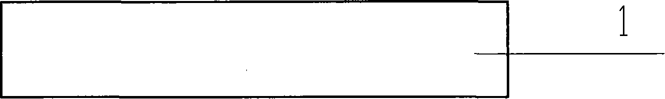
[0027] Such as figure 1 As shown, the substrate 1 adopts a common cleaning method to make the substrate 1 clean and free from contamination, and the moisture on the surface of the substrate 1 is dried in a clean environment at 150 degrees Celsius to 180 degrees Celsius.

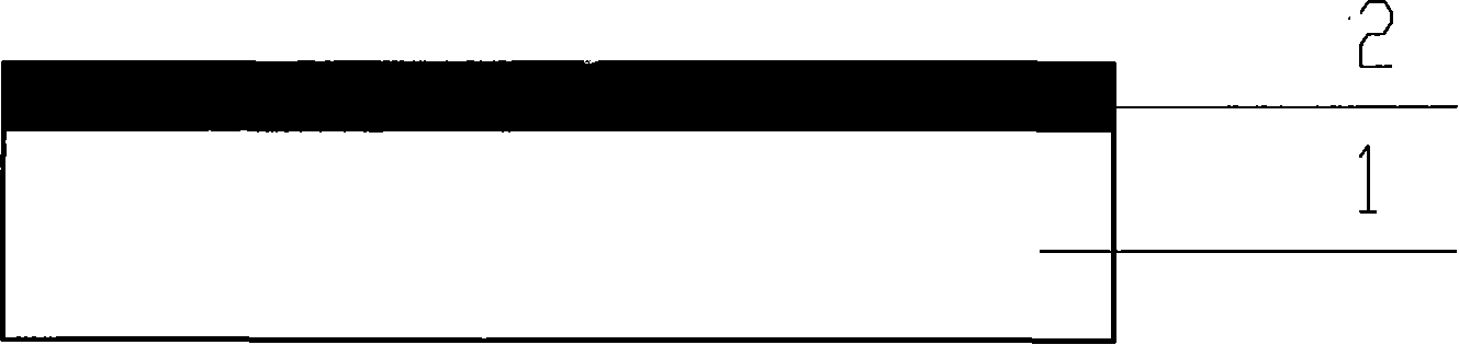
[0028] Such as figure 2 As shown, chemically amplified photoresist 2 for 248nm wavelength photolithography is coated on the substrate. The photoresist 2 has a resolution of 0.2 microns or more and a thickness of about 3000-5000 angstroms. UV135 photoresist is used at 90 degrees Celsius Bake for 60-90 seconds at -130 degrees Celsius.

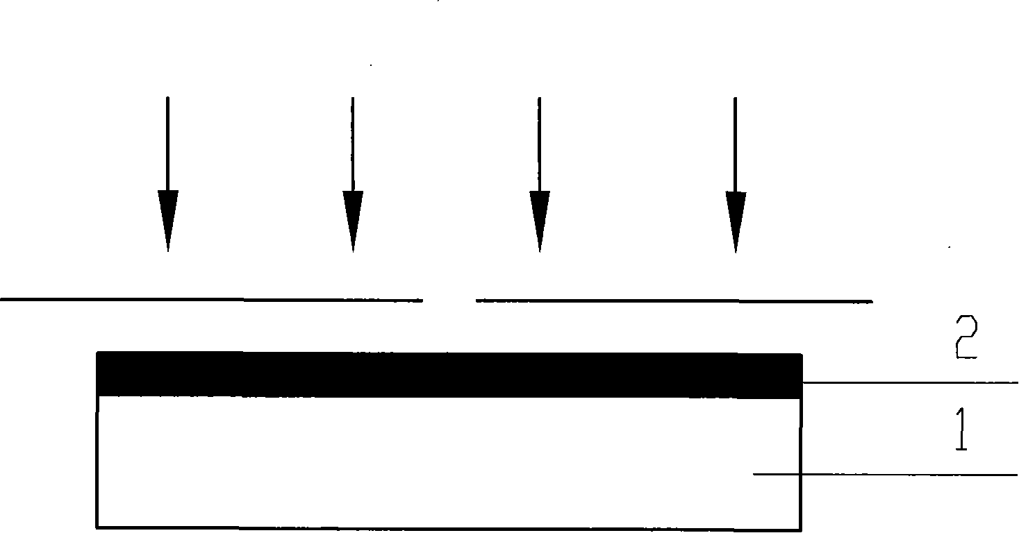
[0029] Such as image 3 As shown, a deep ultraviolet (wavelength 248nm) exposure machine is used for alignment and exposure, and a suitable photoresist plate is selected according to the resolution performance of the lithography machine and the required gate length, ...


PUM


Abstract

The invention discloses a method for manufacturing a T-shaped grate by utilization of deep-UV lithography, comprising the following steps that: a substrate is cleaned and dried and then coated by chemical amplifying deep-UV photoresist; contraposition, alignment, exposure and development are performed by adoption of a deep-UV exposure machine, and a grate root photoresist window graph is formed initially; the photoresist window graph which is formed by exposure is shrunk by adoption of chemical shrinking solution; electron beam slushing compounds are coated; chemical amplifying deep-UV photoresist is coated; contraposition, alignment, exposure and development are performed by adoption of the deep-UV exposure machine; exposure and development are performed by adoption of deep-UV electron beam slushing compounds, and a grate cap photoresist window graph is formed; grate electrode metals are deposited by adoption of the metal evaporation method; the metals are peeled off and the photoresist is stripped, and then manufacture of the T-shaped grate is finished. The method makes a grate root of the T-shaped grate break through the manufacturing limit of superfine lines of a photoetching plate, saves the manufacturing cost of the photoetching plate and simultaneously can realize large-scale deep-submicron processing of compound semiconductor devices.

Description

technical field [0001] The invention belongs to the field of microelectronic processing in semiconductor technology, and in particular relates to a method for manufacturing a "T"-shaped grid by deep ultraviolet lithography. Background technique [0002] In the manufacture of devices in the high-frequency and microwave fields, the shorter the gate length, the higher the operating frequency. Because the high-frequency gain of the device is not only affected by the gate length, but also affected by the gate parasitic parameter gate resistance Rg and gate capacitance Cgs Also big. Reducing the gate length can reduce the gate capacitance Cgs, but it is necessary to ensure that the gate resistance Rg cannot be reduced. In order to solve the contradiction between Rg and Cgs, the "T" gate technology is currently the most effective process. At present, there are many different names, such as: "T"-shaped grid, mushroom-shaped grid, "Γ"-shaped grid, etc., which are visualized accordin...

Claims


Application Information

Patent Timeline
IPC IPC(8): G03F7/00G03F7/039
Inventor 杨中月
Owner THE 13TH RES INST OF CHINA ELECTRONICS TECH GRP CORP
Why Eureka
Try Eureka