Beta -Ga2O3nano lines and gas sensors preparing method, and gas sensing method for realizing quick-speed response
A gas sensor and nanowire technology, applied in the direction of material resistance, etc., to achieve the effect of good stability, simple method and stable performance
- Summary
- Abstract
- Description
- Claims
- Application Information
AI Technical Summary
Problems solved by technology
Method used
Image
Examples
Embodiment 1
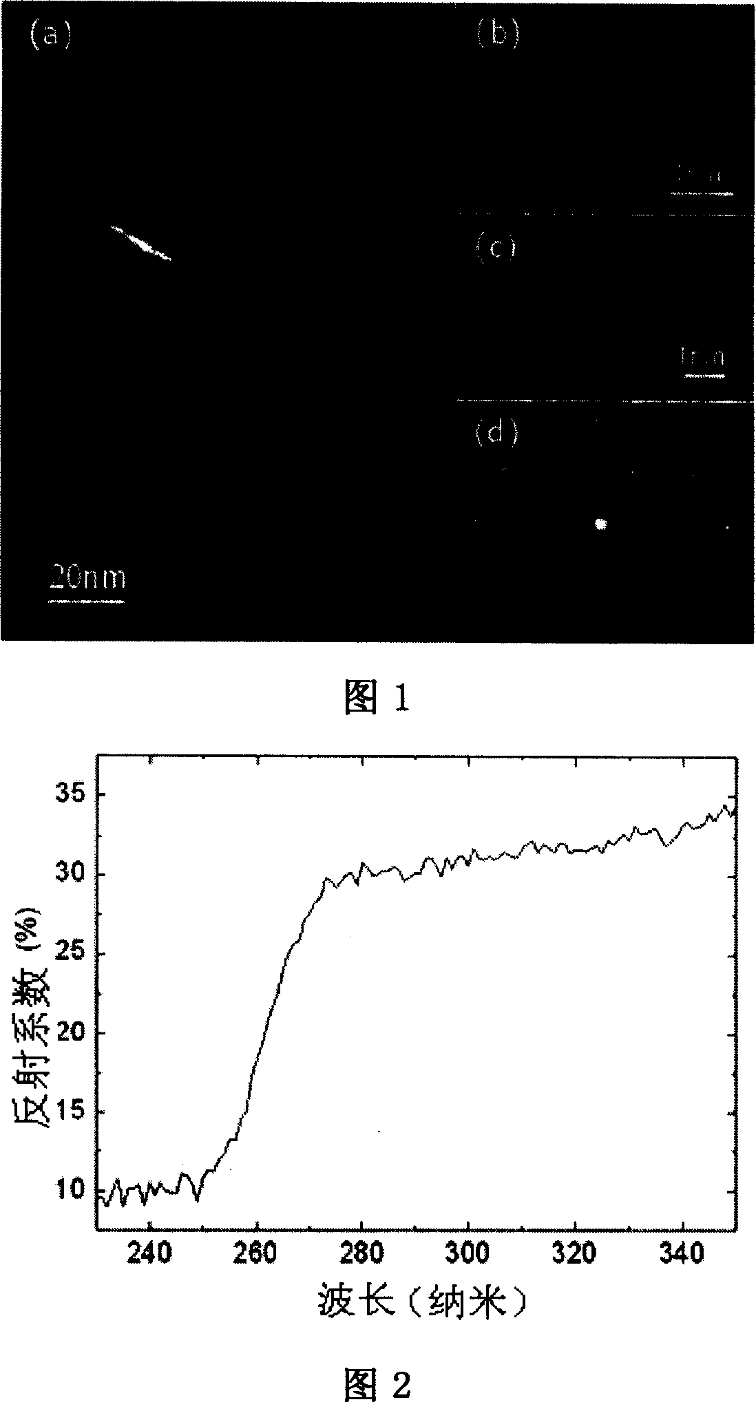
[0045] Example 1: β-Ga 2 o 3 Nanowire preparation method:
[0046] (1) 10 nanometers thick gold film is deposited on the base substrate;
[0047] (2) Put the gallium powder into the boat, place the substrate 1 cm away from the boat, heat and keep warm together;
[0048] (3) Put the alumina boat into the quartz tube, then put the quartz tube into the tube furnace, and then heat the tube furnace to 980°C for 1 hour;
[0049] (4) feed the nitrogen of 400sccm (milliliters / minute) in the heating furnace;
[0050] (5) After the tube furnace is cooled to room temperature, the product—β-Ga 2 o 3 Nanowires are grown on a substrate substrate;
[0051] The base substrate can be an N-type silicon substrate, a P-type silicon substrate, an insulating silicon substrate, or other high-temperature-resistant materials.
[0052] The gold film can be deposited by thermal evaporation, sputtering or electron beam evaporation, and the thickness of the gold film is 10 nanometers.
[0053] The...
Embodiment 2
[0054] Example 2: β-Ga 2 o 3 Preparation of nanowire gas sensor:
[0055] (1) A gold electrode with a thickness of 50nm is deposited by electron beam deposition to a thickness of 500nm, with SiO attached below 2 layer on the silicon substrate.
[0056] (2) The distance between the two electrodes is 1 μm. ;
[0057] (3) placing a single nanowire on the electrode;
[0058] (4) Lead connection. The resulting product is aged for 24 hours.
[0059] The substrates of the two electrodes are realized by photolithography on the ceramic sheet. And it is worth noting that the surface of the nanowires should be very smooth.
Embodiment 3
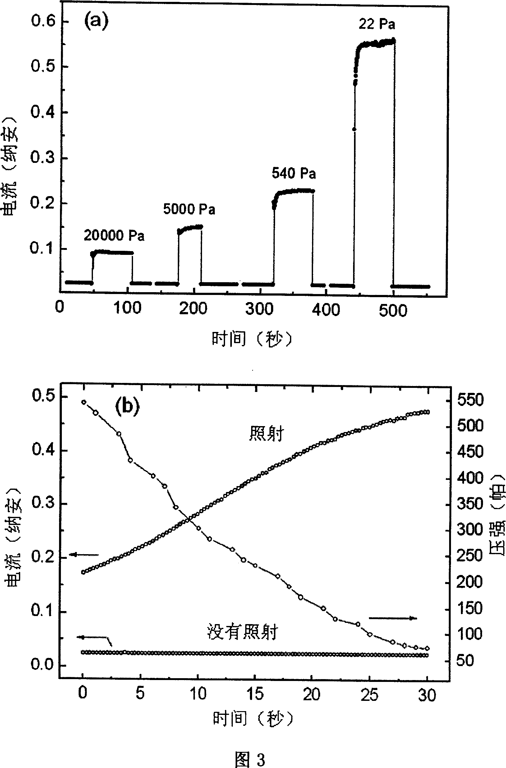
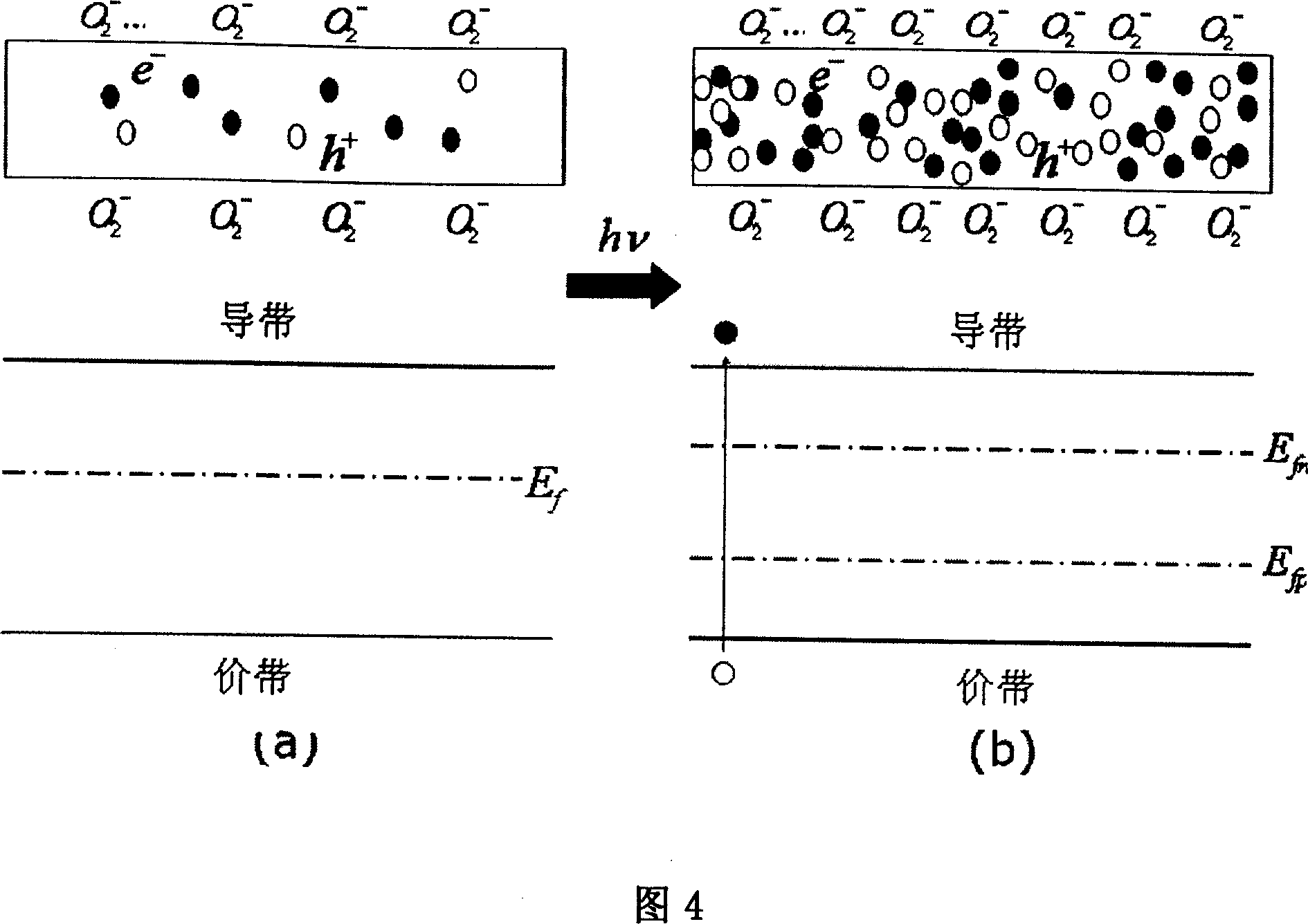
[0060] Embodiment 3: The present invention measures the current passing through the nanowire under different oxygen pressures, under the irradiation of ultraviolet light with a wavelength of 254nm without and with a bias voltage of 20V, and the results are shown in FIG. 3 . Figure 3(a) shows that the current is 26pA under no light condition, and the fluctuation is small under different oxygen pressure. On the contrary, under light conditions, the current rapidly increased to a certain value, reflecting the value of the oxygen pressure in the cavity, the currents were 0.56, 0.23, 0.15 and 0.095nA, and the oxygen pressure in the cavity was 22,540, 5000 and 20000Pa, respectively. The current decreases at a higher oxygen pressure, and the above conclusion is further proved by measuring the current value under the condition of continuously decreasing oxygen pressure [Figure 3(b)]. Comparing in Fig. 3(b), it can be seen that the nanowires are sensitive to oxygen only under irradiati...
PUM
| Property | Measurement | Unit |
|---|---|---|
| thickness | aaaaa | aaaaa |
| thickness | aaaaa | aaaaa |
Abstract
Description
Claims
Application Information
 - R&D
- Intellectual Property
- Life Sciences
- Materials
- Tech Scout
- Unparalleled Data Quality
- Higher Quality Content
- 60% Fewer Hallucinations
Browse by: Latest US Patents, China's latest patents, Technical Efficacy Thesaurus, Application Domain, Technology Topic, Popular Technical Reports.
© 2025 PatSnap. All rights reserved.Legal|Privacy policy|Modern Slavery Act Transparency Statement|Sitemap|About US| Contact US: help@patsnap.com


