Surface-sensitive condenser type gas transducer and manufacturing method thereof
A gas sensor, surface-sensitive technology, applied in semiconductor/solid-state device manufacturing, electrical components, circuits, etc., can solve problems such as dielectric constant change of dielectric layer, complex semiconductor manufacturing process, and influence on capacitance test effect, so as to reduce test voltage , reduce interference and avoid loss
- Summary
- Abstract
- Description
- Claims
- Application Information
AI Technical Summary
Problems solved by technology
Method used
Image
Examples
Embodiment 1
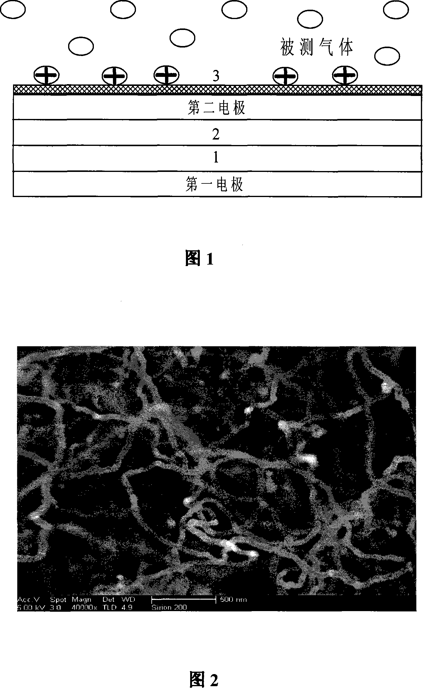
[0041] The fabrication process of the surface-sensitive capacitive gas sensor is as follows: first, the silicon wafer 1 is heavily doped (with a resistivity of 0.001Ω·cm) and used as the first electrode. Then thermally oxidize a 200nm silicon oxide layer on the upper surface of the silicon wafer 1, and then make a layer of gold electrode on the silicon oxide 2 by screen printing, and make a layer of iron electrode on the surface by magnetron sputtering. film.
[0042] Put the finished sample into a tube furnace and use the method of vapor deposition to make a carbon nanotube film. The specific process is: first pass argon gas at a flow rate of 100ml / min for 2 hours to evacuate the air in the tube, and heat it to 600°C. Then flow hydrogen at a flow rate of 100ml / min for 2 hours to reduce the oxidized iron film, and then flow acetylene gas at a flow rate of 15ml / min to start depositing carbon nanotubes. After half an hour, stop heating, turn off acetylene and hydrogen, and cool ...
Embodiment 2
[0044] The manufacturing process of the surface-sensitive capacitive gas sensor is as follows: screen-print a layer of gold paste on the lower surface of the silicon wafer 1, burn it at 820°C for 20 minutes, and then coat a layer of 150nm gold paste on the upper surface of the silicon wafer 1 by sputtering. Silicon oxide 2, on top of the silicon oxide 2, a layer of gold electrode is made by screen printing, and a layer of iron film is made on its surface by magnetron sputtering.
[0045] Put the finished sample into a tube furnace and use the method of vapor deposition to make a carbon nanotube film. The specific process is: first pass argon gas at a flow rate of 200ml / min for 2 hours to evacuate the air in the tube, and heat it to 800°C. Then flow hydrogen at a flow rate of 200ml / min for 1 hour to reduce the oxidized iron film, and then flow acetylene gas at a flow rate of 10ml / min to start depositing carbon nanotubes. After half an hour, stop heating, turn off acetylene and h...
Embodiment 3
[0047] The fabrication process of the surface-sensitive capacitive gas sensor is as follows: first, the silicon wafer 1 is heavily doped (with a resistivity of 0.01 Ω·cm), and then a layer of thermal evaporation is deposited on the lower surface of the silicon wafer 1 under vacuum at 200°C. A gold electrode is then thermally oxidized 100nm silicon oxide 2 on the upper surface of the silicon wafer 1, and a layer of gold electrode is made on the silicon oxide 2 by screen printing.
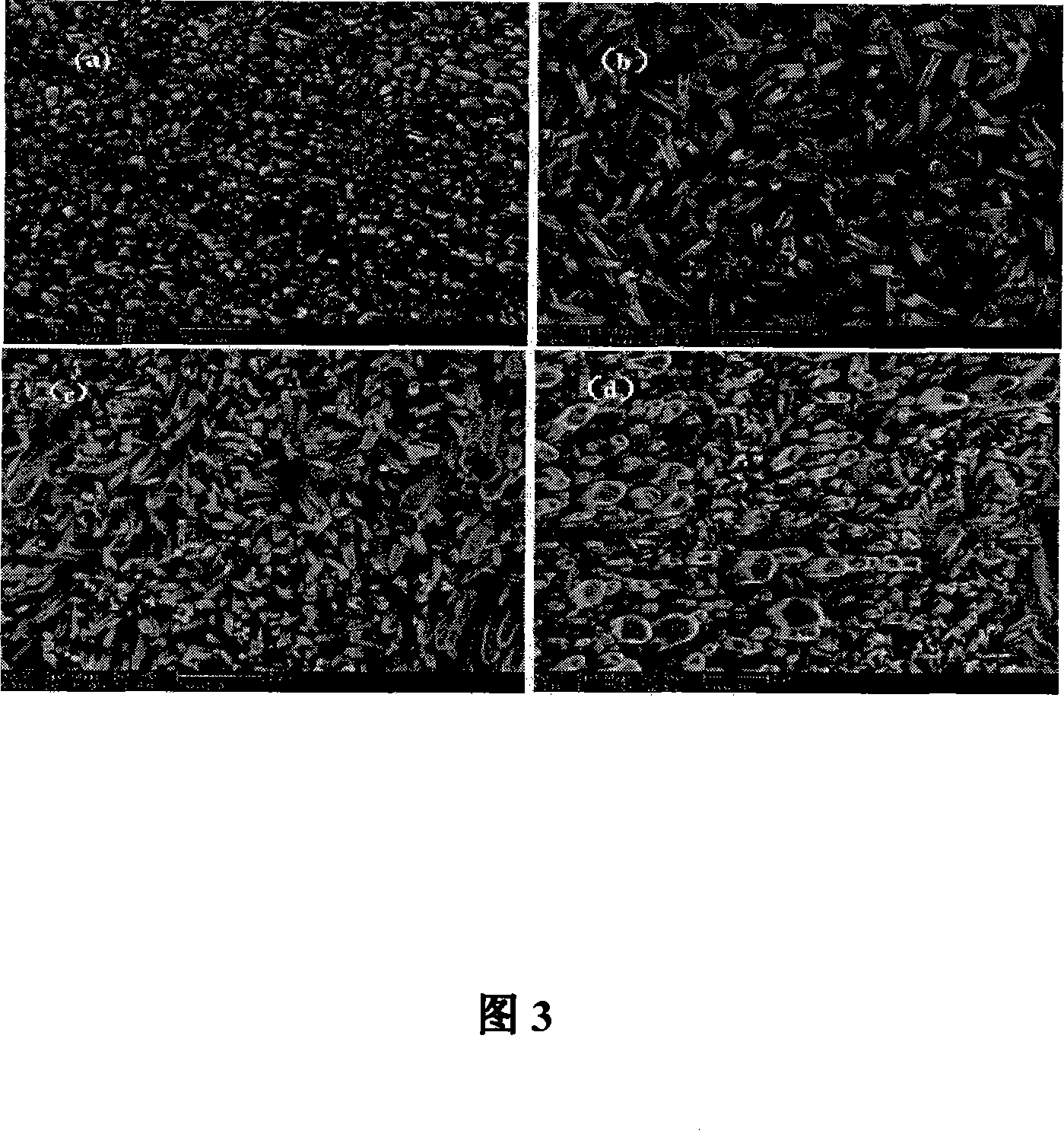
[0048] Zinc oxide nano or microrod arrays were prepared by hydrothermal method, the preparation process is as follows: 30ml 0.5M NaOH solution, 5ml 30% H 2 o 2 Add the solution into an autoclave with a volume of 50ml, stir evenly, add a piece of 1cm×1cm pure and flat zinc sheet, seal it, put it in an oven and heat it to 160-200°C for 1-10 hours. After the reaction, take out the zinc sheet, wash it with deionized water and alcohol, and dry it in a vacuum oven at 40°C for 20 minutes to obtain a zinc o...
PUM
| Property | Measurement | Unit |
|---|---|---|
| Resistivity | aaaaa | aaaaa |
| Resistivity | aaaaa | aaaaa |
| Diameter | aaaaa | aaaaa |
Abstract
Description
Claims
Application Information
 - R&D
- Intellectual Property
- Life Sciences
- Materials
- Tech Scout
- Unparalleled Data Quality
- Higher Quality Content
- 60% Fewer Hallucinations
Browse by: Latest US Patents, China's latest patents, Technical Efficacy Thesaurus, Application Domain, Technology Topic, Popular Technical Reports.
© 2025 PatSnap. All rights reserved.Legal|Privacy policy|Modern Slavery Act Transparency Statement|Sitemap|About US| Contact US: help@patsnap.com


