Direct synthesis process of hydrophobic nanometer silica line with ZnS powder
A technology of silica and nanowires, which is applied in the field of nanomaterials, can solve problems such as complex preparation procedures, high cost, and limited application range, and achieve the effects of simple equipment process, high hydrophobicity, and low price
- Summary
- Abstract
- Description
- Claims
- Application Information
AI Technical Summary
Problems solved by technology
Method used
Image
Examples
Embodiment 1
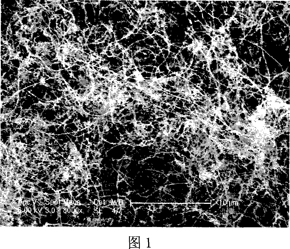
[0027] A ceramic boat equipped with 3 clean silicon wafers (1×1 cm rectangular silicon wafer) was placed in the center of a horizontal quartz tube furnace, and 5 g of solid ZnS powder was fixed on the gas inflow side of the quartz tube. The temperature was raised to a reaction temperature of 1350°C at a rate of 10°C / min. When the temperature starts to rise, argon gas with a gas flow rate of 50ml / min is introduced; at a reaction temperature of 1350°C, the gas flow rate in the chamber is maintained, and the reaction continues for 2 hours. After the reaction, the reaction product is taken out, and a large amount of The disordered silica nanowire sample is shown in Figure 1. It can be seen from the figure that a large number of disordered silica nanowires are produced on the surface of the silicon wafer. The synthesized silica nanowires and 0.05ml of perfluorosilane were sealed and put into a stainless steel tank, and the evaporation reaction was carried out at 150 degrees for 3.0...
Embodiment 2
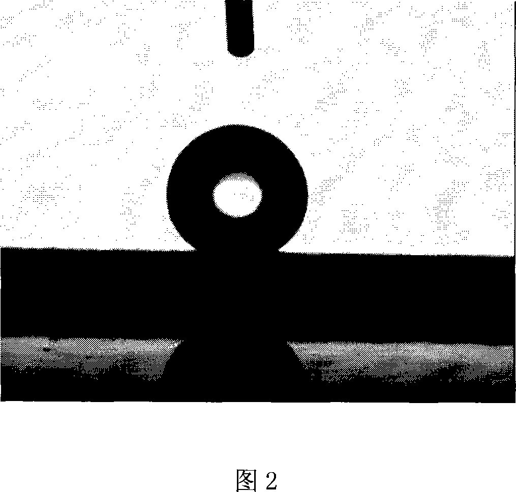
[0029] A ceramic boat equipped with 3 clean silicon wafers (1×1 cm rectangular silicon wafer) was placed in the center of a horizontal quartz tube furnace, and 5 g of solid ZnS powder was fixed on the gas inflow side of the quartz tube. The temperature was raised to a reaction temperature of 1350°C at a rate of 10°C / min. When the temperature starts to rise, argon gas with a gas flow rate of 500ml / min is introduced; at a reaction temperature of 1350°C, the gas flow rate in the chamber is maintained, and the reaction continues for 3 hours. A sample of disordered silica nanowires. Seal the synthesized silica nanowires and 0.1ml of perfluorosilane into a stainless steel tank, and carry out evaporation reaction at 150 degrees for 3.0 hours to obtain a superhydrophobic nanowire with a contact angle of 145 degrees. For silicon oxide nanowires, see Figure 2. It can be seen from the figure that the silicon dioxide nanowire samples show good hydrophobic properties.
Embodiment 3
[0031] A ceramic boat equipped with 3 clean silicon wafers (1×1 cm rectangular silicon wafer) was placed in the center of a horizontal quartz tube furnace, and 5 g of solid ZnS powder was fixed on the gas inflow side of the quartz tube. The temperature was raised to a reaction temperature of 1350°C at a rate of 10°C / min. When the temperature starts to rise, argon gas with a gas flow rate of 200ml / min is introduced; at a reaction temperature of 1350°C, the gas flow rate in the chamber is maintained, and the reaction continues for 5 hours. After the reaction, the reaction product is taken out, and a large amount of A sample of disordered silica nanowires. Seal the synthesized silica nanowires and 0.2ml of perfluorosilane into a stainless steel tank, and carry out evaporation reaction at 150 degrees for 3.0 hours to obtain a superhydrophobic nanowire with a contact angle greater than 140 degrees. Silicon oxide nanowires.
PUM
 Abstract
Description
Claims
Application Information
 - R&D
- Intellectual Property
- Life Sciences
- Materials
- Tech Scout
- Unparalleled Data Quality
- Higher Quality Content
- 60% Fewer Hallucinations
Browse by: Latest US Patents, China's latest patents, Technical Efficacy Thesaurus, Application Domain, Technology Topic, Popular Technical Reports.
© 2025 PatSnap. All rights reserved.Legal|Privacy policy|Modern Slavery Act Transparency Statement|Sitemap|About US| Contact US: help@patsnap.com


