Electronic bubble surface low temperature depositional film manufacture method

A technology of surface deposition and blisters, applied in stacked capacitors, thin film/thick film capacitors, etc., can solve the problems of uneven conductive layer thickness, inaccurate measurement results, damage to electronic blisters, etc., to achieve smooth peeling off and high sensing sensitivity , the effect of not easy to fall off

Inactive Publication Date: 2007-10-24
YANGZHOU UNIV
View PDF0 Cites 0 Cited by
  • Summary
  • Abstract
  • Description
  • Claims
  • Application Information

AI Technical Summary

Problems solved by technology

However, the thickness of the conductive layer produced by this method is very uneven, which is likely to cause large measurement errors, resulting in inaccurate measurement results, and at the same time damage the electronic blisters, making the measurement impossible

Method used


Image

  • Electronic bubble surface low temperature depositional film manufacture method
  • Electronic bubble surface low temperature depositional film manufacture method
  • Electronic bubble surface low temperature depositional film manufacture method

Examples


Embodiment Construction

[0023] First clean the glass surface:

[0024] Soak in a mixture of analytical ethanol and ether at a ratio of 3:1 to remove oil stains; then use ultrasonic cleaning; finally wipe dry with analytical ethanol and dry the glass surface with a dry hot air blower and a flat nozzle.

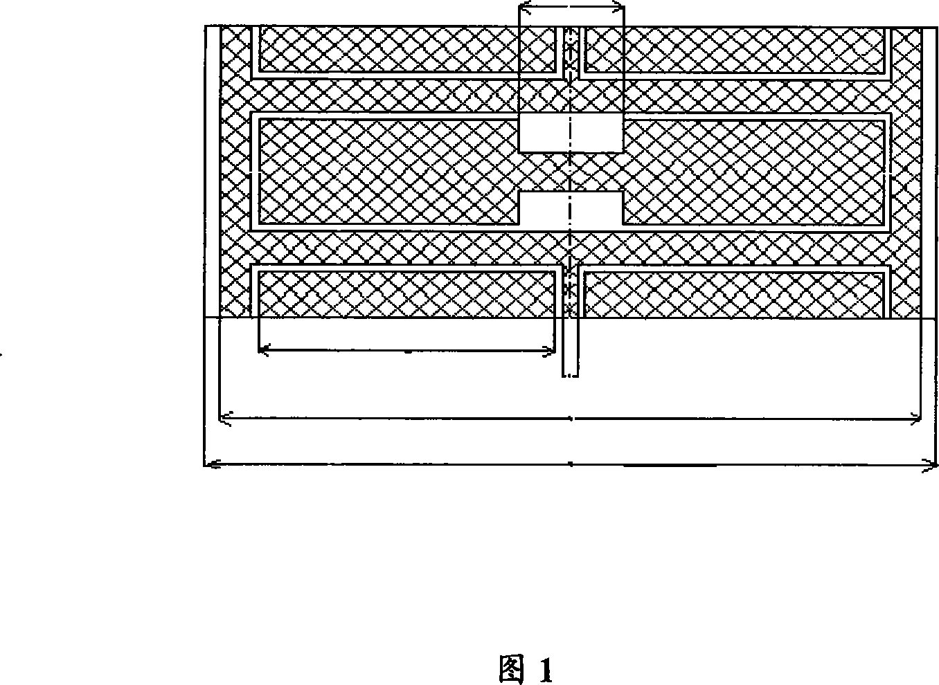
[0025] Apply photosensitive glue on the blank part of the surface of the electronic blister and cure it with ultraviolet light.

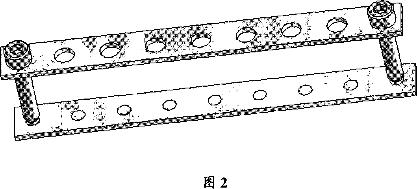
[0026] Install the fixture:

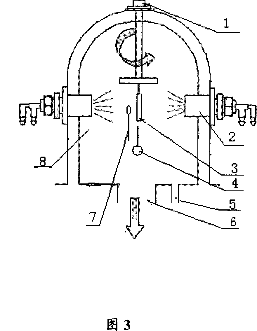
[0027] As shown in Figure 2, put the electronic water bubbles into the holes of the fixture 4 one by one, clamp the fixture 4 and put it into the vacuum chamber 8, and connect it to the rotating motor 1;

[0028] DC magnetron sputtering:

[0029] As shown in Figure 3, put the clamp 3 shown in Figure 2 into the vacuum chamber 8 after being clamped, and vacuumize the vacuum chamber 8 through the vacuum port 6 to obtain a background vacuum degree of 10 -3 Pa, then fill argon into the vacuum chamber 8 through the argon gas inlet 5; control the a...


PUM


Abstract

The related preparation method for capacitance film on surface of electronic bubble comprises: cleaning and drying the bubble surface, coating photoresist on the blank surface, curing with UV-ray, putting into holder hole to put in vacuum chamber together, rotating, vacuum-pumping to 10-3Pa, filling Ar gas to make 0-10Pa vacuum degree; applying voltage on the target to form a plasma area between the target and holder; setting the film thickness, plating Ni80Cr2O bottom film on bubble surface, adjusting the sputtering power, depositing Cu film, and removing the resist. This invention balance thickness of conductive layer, reduces measurement error, improves compensation precision of capacitive reactance and the sensitivity.

Description

technical field [0001] The invention relates to a method for preparing a capacitor film deposited at low temperature on the surface of an electronic water bubble. Background technique [0002] Since the e-bubble contains a mixture of ethanol and ethanol, it is very difficult to deposit a capacitive film on its surface, and the e-bubble is prone to bursting after being heated, resulting in failure or scrapping. [0003] Before the present invention, the existing method is to use very thin copper skin or copper sheet to paste on the surface of the electronic bubble, or to use the method of brushing conductive glue or silver paste to form a capacitance compensation circuit. However, the thickness of the conductive layer produced by this method is very uneven, which easily causes large measurement errors, resulting in inaccurate measurement results, and at the same time damages the electronic blisters, making the measurement impossible. Contents of the invention [0004] The ...

Claims


Application Information

Patent Timeline
Patent Type & Authority Applications(China)
IPC IPC(8): H01G4/33
Inventor 陈荣发赵毅红
Owner YANGZHOU UNIV
Why Eureka
Try Eureka