Chemical reaction apparatus and power supply system
A technology of chemical reaction and power supply system, applied in chemical/physical/physicochemical fixed reactors, inorganic chemistry, electrochemical generators, etc., can solve the problems of increasing heat energy loss and deterioration of energy utilization, so as to improve energy utilization, Effect of suppressing heat loss and improving power generation efficiency
- Summary
- Abstract
- Description
- Claims
- Application Information
AI Technical Summary
Problems solved by technology
Method used
Image

Examples
no. 1 example
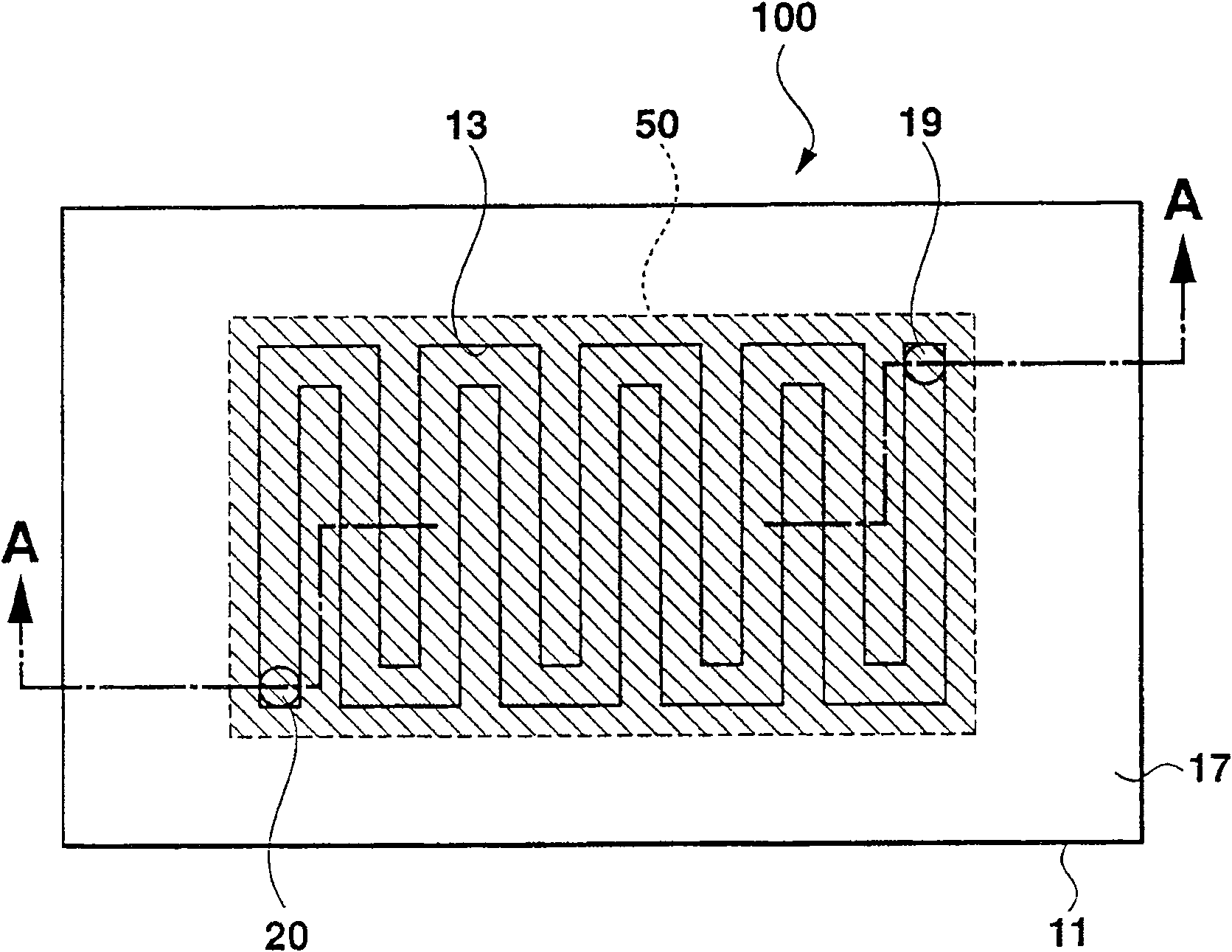
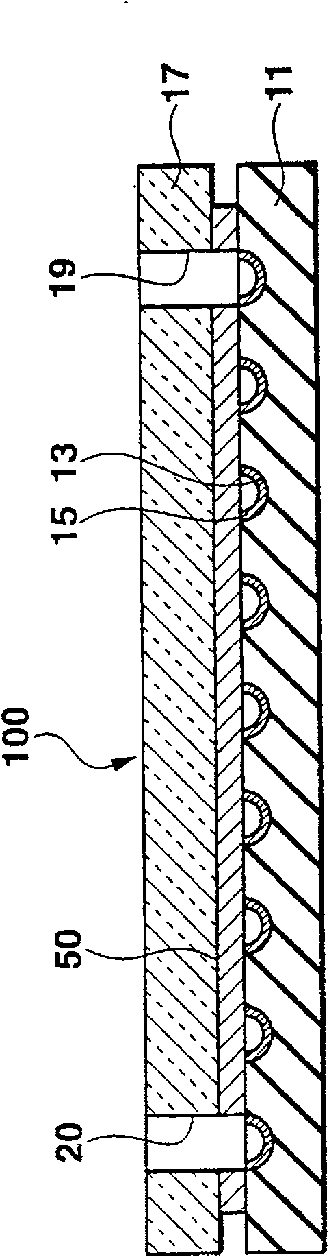
[0053] figure 1 It is a broken sectional view of the first embodiment of the chemical reaction device of the present invention. figure 2 It is a sectional view taken along the A-A line of the chemical reaction device.
[0054] The chemical reaction device 100 of the first embodiment of the present invention includes rectangular plate-shaped first and second substrates 11 and 17 stacked and bonded via a thin film heater 50 . The first substrate 11 is, for example, a silicon substrate, and the second substrate 17 is, for example, a glass substrate. For example, the length of the first substrate 11 is about 25 mm, the width is about 17 mm, and the thickness is about 0.6 to 1 mm. In addition, the thickness of the second substrate 17 is, for example, about 0.7 mm, and the length and width are the same as those of the first substrate.
[0055] In a plane of the first substrate 11, a zigzag-shaped reaction flow path 13 having a predetermined groove-like cross-section and having ...
no. 2 example
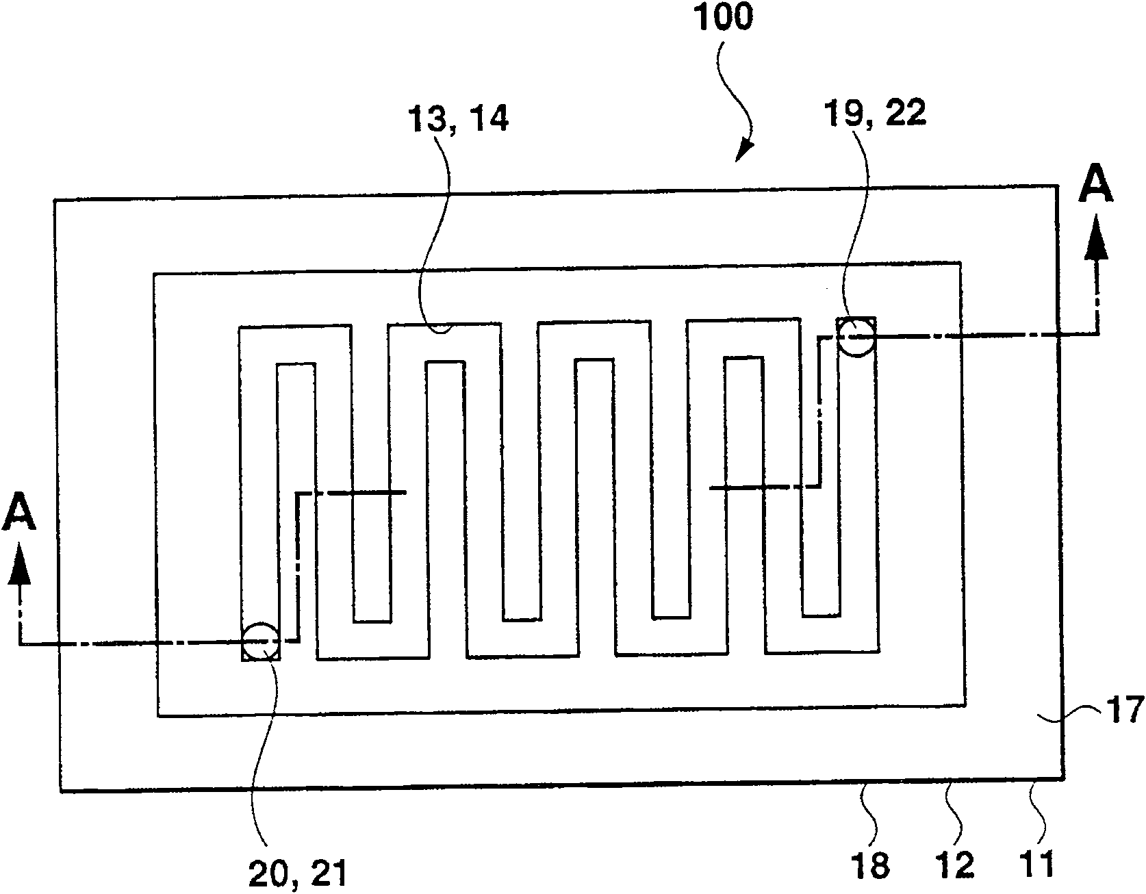
[0063] image 3 It is a broken sectional view of the second embodiment of the chemical reaction device 100 of the present invention. Figure 4 is a cross-sectional view taken along line A-A of the chemical reaction device 100.
[0064] The chemical reaction device 100 of the second embodiment has first and second substrates 11 and 12 adjacent to each other. The first and second substrates 11, 12 are rectangular plate-shaped substrates made of a semiconductor material such as silicon. For example, the first and second substrates 11 and 12 are bonded by an adhesive, but they may simply be in close contact with each other without any adhesive. The dimensions of the first and second substrates 11 and 12 are, for example, about 25 mm in length, about 17 mm in width, and about 0.6 to 1 mm in thickness.
[0065] Utilize the microtopography technology that develops in semiconductor manufacturing technology, on one surface or upper surface of first substrate 11 and on the other surf...
no. 3 example
[0085] Figure 8 is a sectional view showing an apparatus as a third embodiment of the chemical reaction apparatus of the present invention.
[0086] In the third embodiment, if the reactive fluid supplied to the first flow path 13 of the first substrate 11 contains a combustible component, the reactive fluid is supplied to the inlet 19 of the third substrate 17 . Further, as a combustion fluid, the reaction fluid and oxygen obtained from the atmosphere are supplied to the inlet 21 of the third substrate 18 .
[0087] For example, when the chemical reaction device 100 is applied to a conversion unit of a power supply system using a fuel unit described later, and is supplied as a reaction fluid by evaporating methanol aqueous solution (CH 3 OH+H 2 O) when the fuel gas for power generation is produced, the fuel gas for power generation contains combustible components (hydrogen), so the structure of the third embodiment is suitable for application. Therefore, power generation ...
PUM
| Property | Measurement | Unit |
|---|---|---|
| length | aaaaa | aaaaa |
| width | aaaaa | aaaaa |
| thickness | aaaaa | aaaaa |
Abstract
Description
Claims
Application Information
 - Generate Ideas
- Intellectual Property
- Life Sciences
- Materials
- Tech Scout
- Unparalleled Data Quality
- Higher Quality Content
- 60% Fewer Hallucinations
Browse by: Latest US Patents, China's latest patents, Technical Efficacy Thesaurus, Application Domain, Technology Topic, Popular Technical Reports.
© 2025 PatSnap. All rights reserved.Legal|Privacy policy|Modern Slavery Act Transparency Statement|Sitemap|About US| Contact US: help@patsnap.com