Metal oxide semiconductor device grid preparation method

A technology of oxide semiconductor and manufacturing method, applied in semiconductor/solid-state device manufacturing, semiconductor devices, electrical components, etc., can solve problems such as thinning, polysilicon layer damage thickness, etc., to improve reliability, reduce thermal budget, reduce damage effect

Active Publication Date: 2009-07-22
SEMICON MFG INT (SHANGHAI) CORP +1
View PDF5 Cites 0 Cited by
  • Summary
  • Abstract
  • Description
  • Claims
  • Application Information

AI Technical Summary

Problems solved by technology

[0009] Therefore, the object of the present invention is to provide a method for manufacturing the gate of a metal oxide semiconductor device, so as to solve the problem that the polysilicon layer is damaged and the thickness is reduced in the existing gate manufacturing process

Method used


Image

  • Metal oxide semiconductor device grid preparation method
  • Metal oxide semiconductor device grid preparation method
  • Metal oxide semiconductor device grid preparation method

Examples


Embodiment Construction

[0029] In order to make the above objects, features and advantages of the present invention more comprehensible, specific implementations of the present invention will be described in detail below in conjunction with the accompanying drawings.

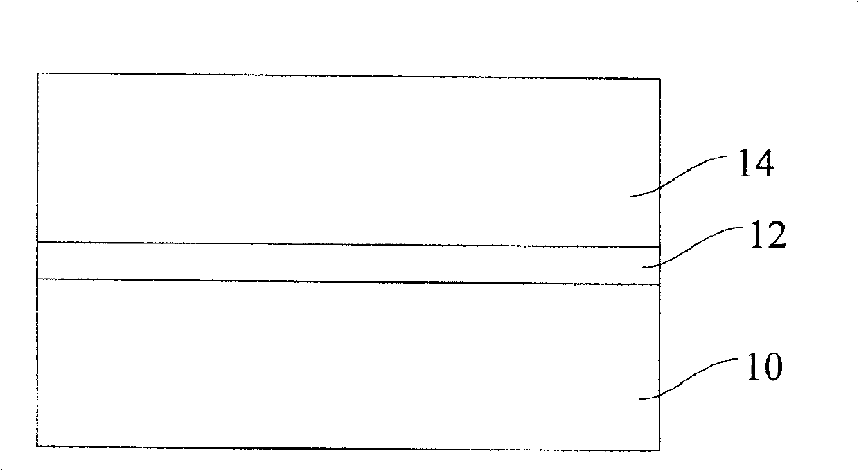
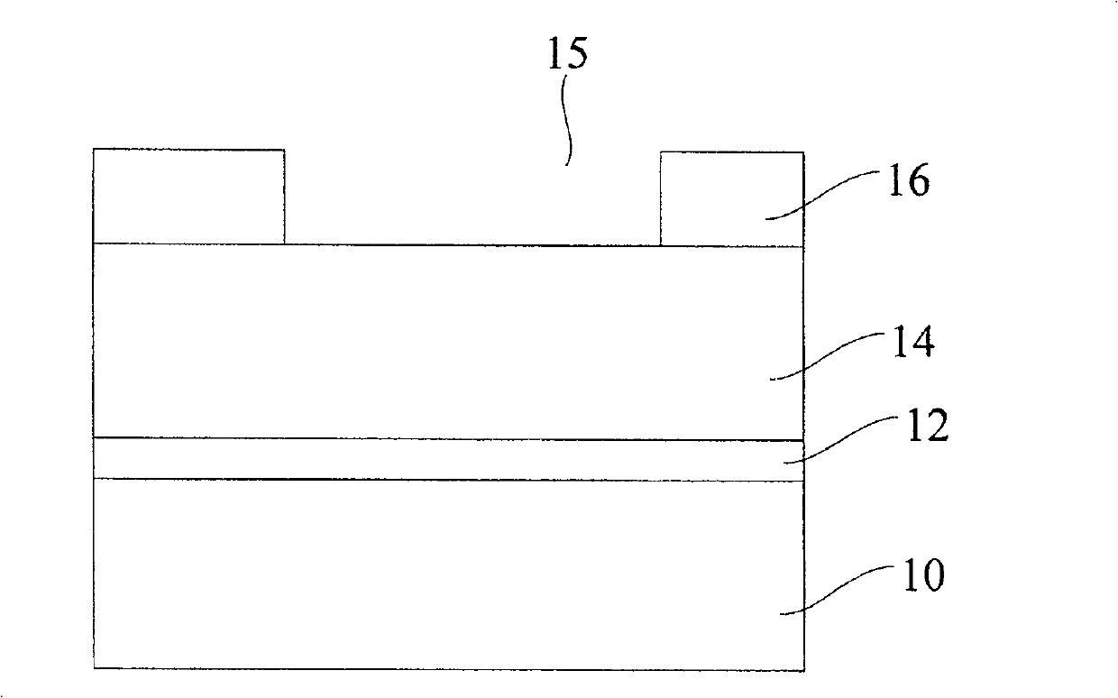
[0030] Figure 6 It is a flowchart of an embodiment of a method for manufacturing a metal oxide semiconductor device gate according to the present invention. Such as Figure 6 As shown, firstly, a semiconductor substrate is provided, and the semiconductor substrate is one of polycrystalline silicon, single crystal silicon, amorphous silicon, silicon-on-insulator, silicon-germanium composition, and gallium arsenide. Doping N-type impurities or P-type impurities into the semiconductor substrate to form a conductive channel of the device. The surface of the semiconductor substrate has a thin oxide layer, the thickness of the oxide layer is 1 to 100 nm, and the formation method of the oxide layer is high temperature thermal oxidation or ...


PUM

PropertyMeasurementUnit
thicknessaaaaaaaaaa

Abstract

The invention relates to a method for manufacturing a grid of a semiconductor part with a metal oxide, which comprises the following steps: a heteromorphic silicon layer is formed on a basement of a semiconductor; an overburden layer is formed on the heteromorphic silicon layer; an adulteration and an annealing processes are carried out to the heteromorphic silicon layer; a lithography glue layer is spin-coated on the overburden layer and is graphic to form a grid pattern; the overburden layer and the heteromorphic silicon layer which are not covered by the grid pattern are sculptured. The adulteration to the heteromorphic silicon layer is carried out after the overburden layer is formed through the method of the invention, which can prevent the heteromorphic silicon layer from being damaged when an ion form ashing and wet cleaning processes are carried out.

Description

technical field [0001] The invention relates to the technical field of semiconductor manufacturing, in particular to a method for manufacturing a gate of a metal oxide semiconductor device. Background technique [0002] In the manufacturing process of metal oxide semiconductor devices, the manufacturing process of the gate plays an important role, representing the technological level of the entire semiconductor manufacturing process. Since the parameters such as the line width and resistivity of the gate directly affect the response rate and power consumption of the formed device, semiconductor manufacturing and R&D engineers take reducing the line width and resistivity of the gate as the main task. For example, the US patent No. US6875668B2 reduces the bottom line width of the gate by selective etching; the Chinese patent No. 97126460.0 forms the gate by forming doped metal silicide on the polysilicon, reducing the gate width. The resistivity of the electrode, the publishe...

Claims


Application Information

Patent Timeline
Patent Type & Authority Patents(China)
IPC IPC(8): H01L21/28H01L21/336
Inventor 张海洋马擎天陈海华
Owner SEMICON MFG INT (SHANGHAI) CORP
Why Eureka
Try Eureka