TV set and image display device
An image display device and a technology for displaying images, applied in image/graphic display tubes, televisions, color televisions, etc.
- Summary
- Abstract
- Description
- Claims
- Application Information
AI Technical Summary
Problems solved by technology
Method used
Image
Examples
example 1
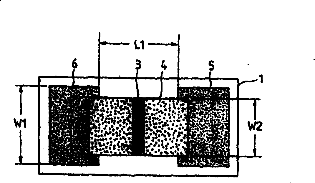
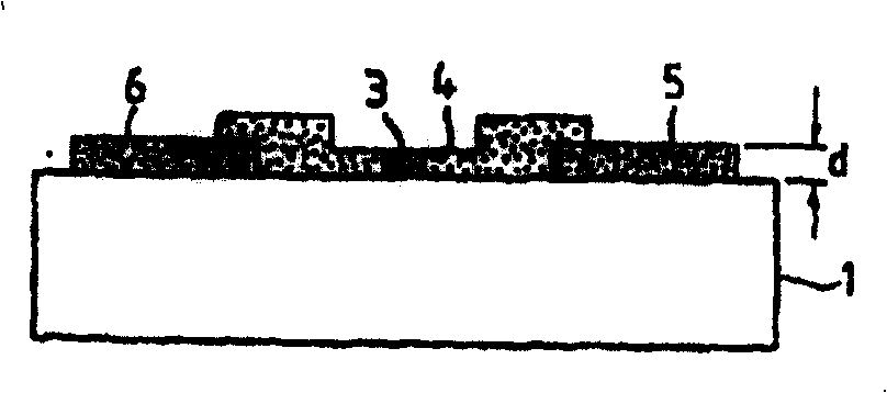
[0132] Example 1. The basic structure of the device used in this example and Figure 1A floor plan and Figure 1B The same as shown in the (section) figure. Four identical devices are formed on a substrate 1 . Notice Figure 11 The meaning of the labels in and Figure 1A , 1B The same reference numerals represent the same elements.
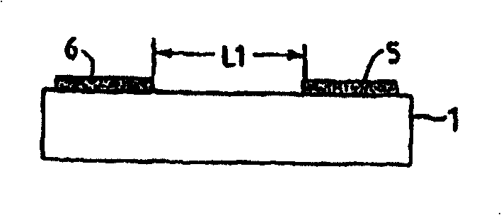
[0133] The method of making this device and Figures 2A to 2C The method of explanation is basically the same.
[0134] Refer below Figure 1A , 1B and Figures 2A to 2C The basic structure of the device and its fabrication method are described.
[0135] see Figure 1A Figure 1B , The sample of the prepared electron-emitting device includes a substrate 1, a pair of device electrodes 5, 6, and a thin film 4 including an electron-emitting region 3.
[0136] see Figure 1A , 1B and 2A to 2C, the method of fabricating the device based on the experiments performed on this sample is described as follows:
[0137] Step A:
[0138] After...
example 2
[0159] In this example, a large number of surface conduction electron-emitting devices are arranged in a simple matrix to form an image forming apparatus.
[0160] Figure 13 is a partially enlarged plan view of the electron source substrate of the device. Figure 14 Yes Figure 13 The enlarged schematic diagram of the cross section of the substrate along the A-A line. pay attention to Figure 13 , 14, 15A to 15D and 16E to 16H the same reference numerals represent the same elements. In this way, reference numerals 81, 82, and 83 respectively represent the substrate, the X-direction wiring corresponding to the external terminal DXm (also called the lower wiring), and the y-directional wiring corresponding to the external terminal Dyn (also called the upper wiring). ), and the reference numeral 4 represents the thin film comprising the electron emission region, the reference numerals 5 and 6 represent a pair of device electrodes, and the reference numerals 141 and 142 repr...
example 3
[0195] Samples of electron-emitting devices were prepared as described in Example 1.
[0196] Each of the manufactured electron-emitting devices had a device width W2 of 300 μm, a thin film 2 for the electron-emitting region of the device had a thickness of 10 nm, and a resistance per unit area of 5×10 4 Ω / port. In addition, the device used was the same as the corresponding device in Example 1.
[0197] Then position a metering system as shown in Figure 3, and use the magnetic levitation pump to pump air from the inside to reach 2×10 -8 Torr vacuum. Next, a voltage is applied to the device electrodes 5 and 6 using a power source 31 that supplies a device voltage Vf to the device, and the device is subjected to electric forming (electric forming treatment). Figure 4B The voltage waveforms used for the electroforming process are shown in .
[0198] exist Figure 4B Among them, T1 and T2 respectively represent the pulse width and pulse interval of the applied pulse voltag...
PUM
 Abstract
Description
Claims
Application Information
 - R&D Engineer
- R&D Manager
- IP Professional
- Industry Leading Data Capabilities
- Powerful AI technology
- Patent DNA Extraction
Browse by: Latest US Patents, China's latest patents, Technical Efficacy Thesaurus, Application Domain, Technology Topic, Popular Technical Reports.
© 2024 PatSnap. All rights reserved.Legal|Privacy policy|Modern Slavery Act Transparency Statement|Sitemap|About US| Contact US: help@patsnap.com


