Electron-emitting device and image display apparatus
An electron emission and image display technology, applied in image/graphic display tubes, electrical components, discharge tube/lamp parts, etc., can solve problems such as fluctuations in electron emission, difficulty in obtaining high-definition display images, and brightness fluctuations
- Summary
- Abstract
- Description
- Claims
- Application Information
AI Technical Summary
Problems solved by technology
Method used
Image
Examples
no. 1 example
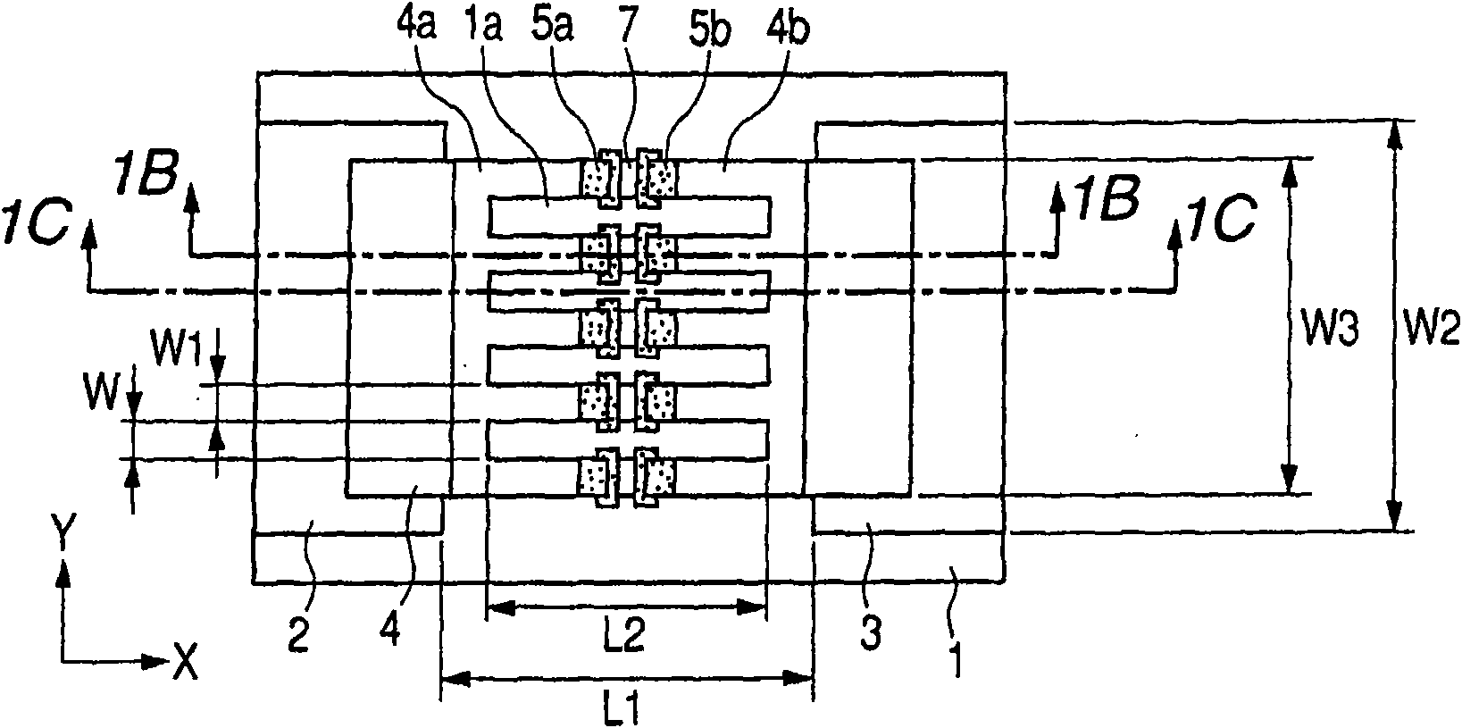
[0035] First, refer to Figure 1A to Figure 1D The basic configuration of the most typical embodiment of the first electron-emitting device of the present invention will be described. Figure 1A is a schematic plan view showing a typical configuration in this embodiment. Figure 1B is along Figure 1A A schematic cross-sectional view taken on line 1B-1B. Figure 1C is along Figure 1A A schematic cross-sectional view taken by line 1C-1C. Figure 1D is along Figure 1APerspective view cut by line 1C-1C.
[0036] In the present invention, it is assumed that the facing direction of the device electrodes 2 and 3 is the X direction, the direction perpendicular to the facing direction (the direction along the gap 7 between the device electrodes) is assumed to be the Y direction, and the substrate The normal direction of 1 is the Z direction.
[0037] The device electrodes 2 and 3 are arranged on the insulating substrate 1 so as to be separated from each other by a distance L1. T...
no. 2 example
[0084] will refer to Figure 4A to Figure 4D The basic configuration of the most typical embodiment of the second electron-emitting device of the present invention is described. Figure 4A is a schematic plan view showing a typical configuration in this embodiment. Figure 4B is along Figure 4A A schematic cross-sectional view taken by line 4B-4B. Figure 4C is along Figure 4A A schematic cross-sectional view taken by line 4C-4C. Figure 4D is along Figure 4A A perspective view cut by line 4C-4C.
[0085] In the first embodiment, the conductive films 4 a and 4 b are arranged to face each other through the recess 1 a formed in the insulating substrate 1 . However, in the second embodiment, on the contrary, the conductive films 4a and 4b are arranged in the concave portion, and the opening portions of the conductive films 4a and 4b are arranged in a region adjacent to the concave portion 1a in the Y direction (in the area of the substrate 1 on the surface). In this ...
PUM
 Abstract
Description
Claims
Application Information
 - R&D Engineer
- R&D Manager
- IP Professional
- Industry Leading Data Capabilities
- Powerful AI technology
- Patent DNA Extraction
Browse by: Latest US Patents, China's latest patents, Technical Efficacy Thesaurus, Application Domain, Technology Topic, Popular Technical Reports.
© 2024 PatSnap. All rights reserved.Legal|Privacy policy|Modern Slavery Act Transparency Statement|Sitemap|About US| Contact US: help@patsnap.com


