Projection exposure apparatus having an off-axis alignment system and method of alignment therefor
a technology of projection exposure and off-axis alignment, which is applied in the direction of photomechanical equipment, instruments, material analysis through optical means, etc., can solve the problems of difficult to implement the direction of mark detection, limit the improvement of the accuracy with which to measure the base line value, and limit the increase in the speed with which to execute the base line measurement process. achieve the effect of reducing the throughput and high correction speed
- Summary
- Abstract
- Description
- Claims
- Application Information
AI Technical Summary
Benefits of technology
Problems solved by technology
Method used
Image
Examples
first embodiment
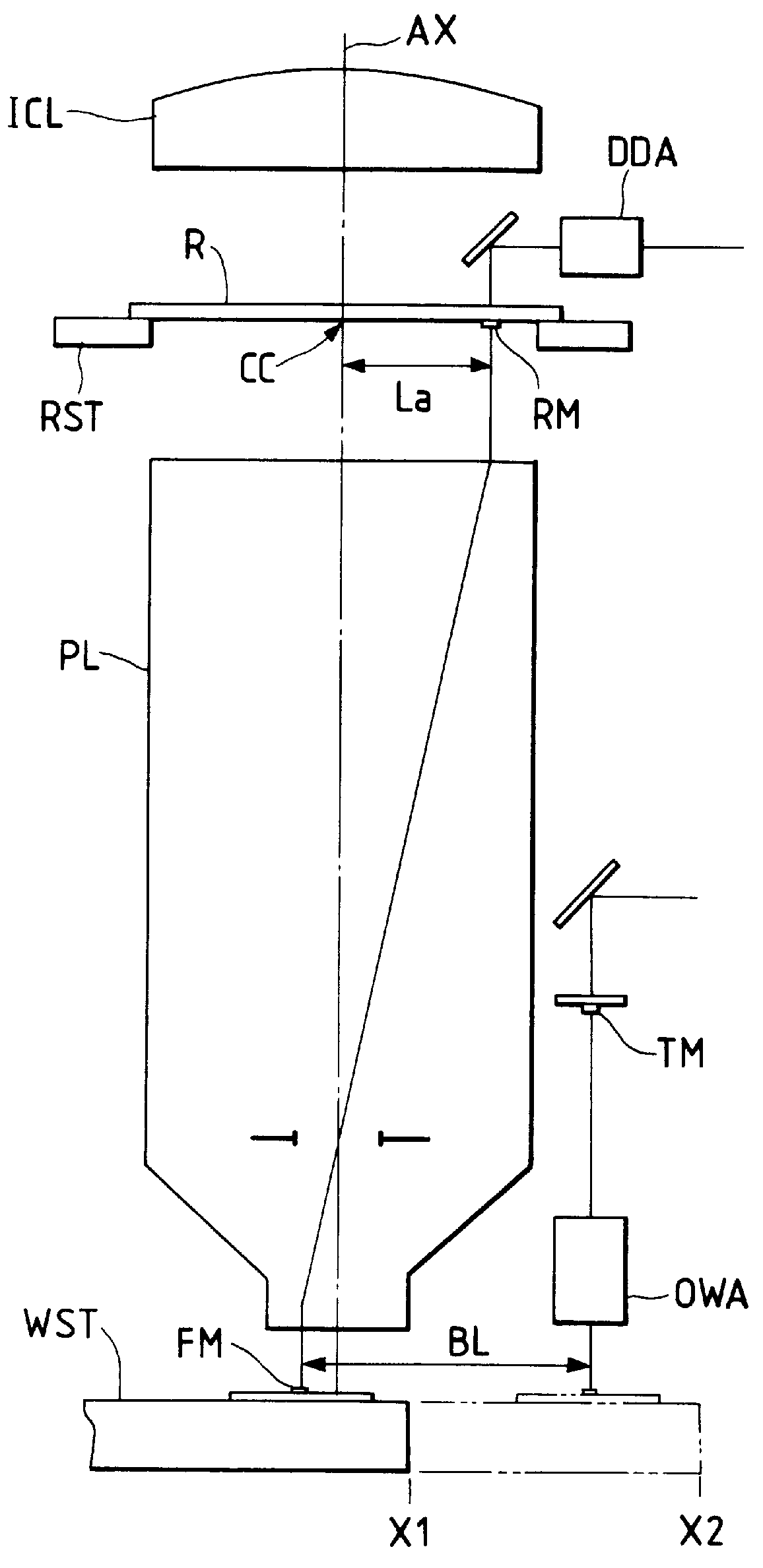
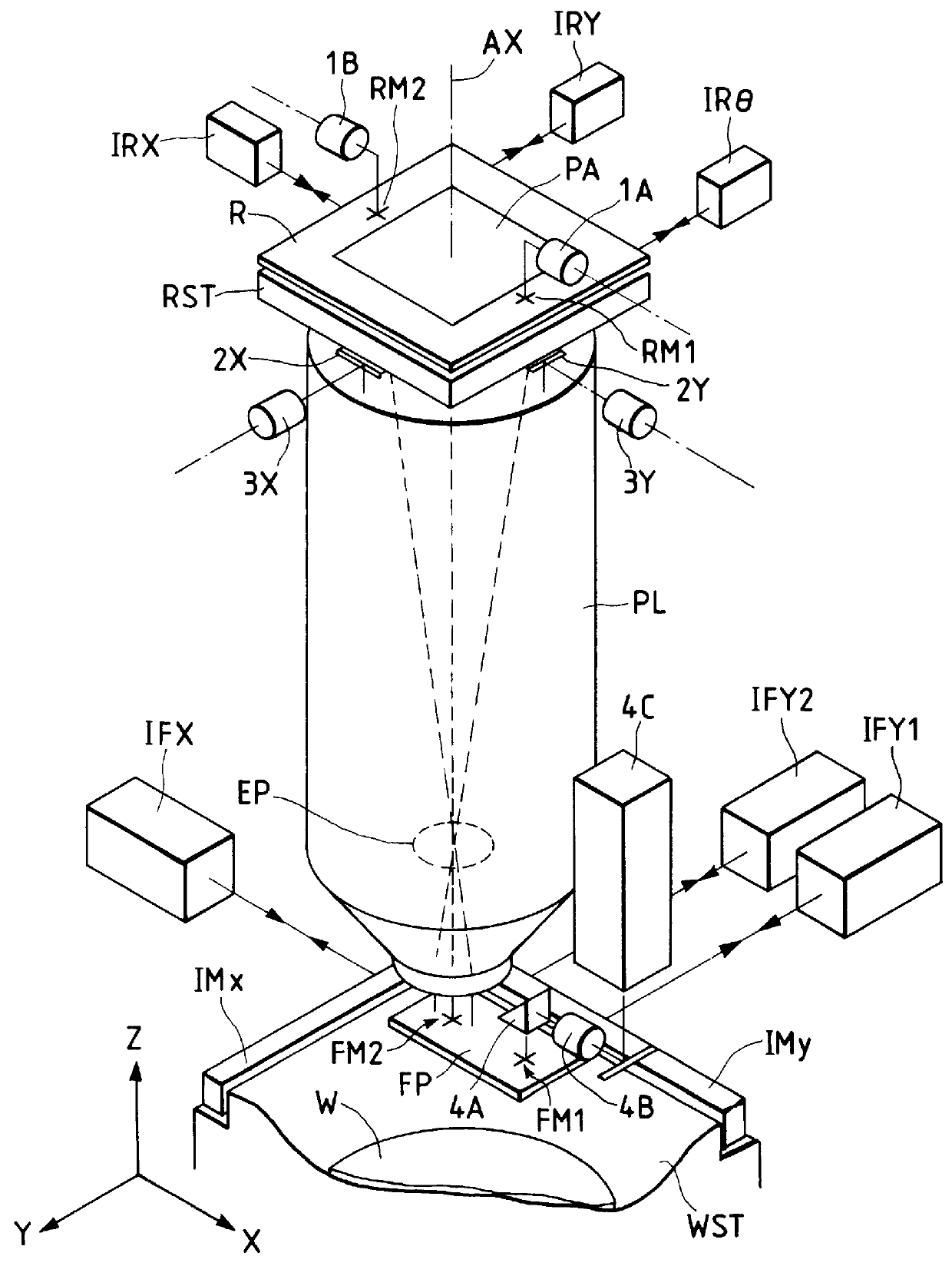
FIG. 2 is a perspective view illustrating the structure of a projection exposure apparatus according to the present invention, in which the same reference marks are given to the members which are the same as those appearing in FIG. 1. In FIG. 2, there are provided on the reticle R, a pattern area PA with the circuit patterns to be exposed on the wafer, and the reticle marks RM.sub.1 and RM.sub.2 for alignment. These reticle marks RM.sub.1 and RM.sub.2 are photoelectrically detected through the object lenses 1A and 1B of a first TTL alignment system respectively. Also, a reticle stage RST is movably driven by a motor and others of the driving system, which is not shown in FIG. 2, in two dimensional (X, Y, and .theta.) directions and its driving amounts or driving positions are sequentially detected by three laser interferometers IRX, IRY, and IR.theta.. The rotational driving amount of the reticle stage RST around the coordinate axis Z (which is parallel with the optical axis AX) is ...
second embodiment
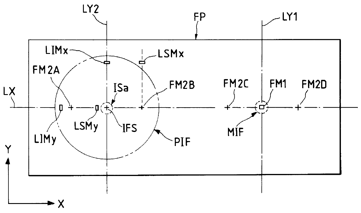
FIG. 23 illustrates the structure of the a projection exposure apparatus according to the present invention. FIG. 24 is a block diagram showing the arrangements of the wafer stage and laser interferometers and the control system of the apparatus shown in FIG. 23.
In FIG. 23, a reticle R having a predetermined pattern area PA is held on a reticle stage which is not shown, and is positioned so that the optical axis AX of a project lens PL can pass through the center point of the pattern area PA. This reticle stage is finely driven by a motor in the direction X, direction Y, and direction .theta. (rotation around the optical axis AX) to drive the reticle R for the alignment with the wafer through the projection lens PL (die by die alignment) or for the alignment of the reticle R itself with respect to the apparatus (reticle alignment). Also, in four locations in the circumference of the pattern area PA of the reticle R, the reticle alignment (or die by die alignment) marks RMx.sub.1, RM...
PUM
| Property | Measurement | Unit |
|---|---|---|
| angle | aaaaa | aaaaa |
| band width | aaaaa | aaaaa |
| length | aaaaa | aaaaa |
Abstract
Description
Claims
Application Information
 - R&D
- Intellectual Property
- Life Sciences
- Materials
- Tech Scout
- Unparalleled Data Quality
- Higher Quality Content
- 60% Fewer Hallucinations
Browse by: Latest US Patents, China's latest patents, Technical Efficacy Thesaurus, Application Domain, Technology Topic, Popular Technical Reports.
© 2025 PatSnap. All rights reserved.Legal|Privacy policy|Modern Slavery Act Transparency Statement|Sitemap|About US| Contact US: help@patsnap.com


