Group 13 nitride crystal and group 13 nitride crystal substrate
a nitride crystal and substrate technology, applied in the direction of crystal growth process, polycrystalline material growth, chemistry apparatus and processes, etc., can solve the problems of high manufacturing cost, difficult to prolong the lifetime of emitting devices, and affecting device properties
- Summary
- Abstract
- Description
- Claims
- Application Information
AI Technical Summary
Benefits of technology
Problems solved by technology
Method used
Image


Examples
examples
[0232]Examples will be shown below to describe the present invention in more detail. However, the invention is not limited to these Examples. Reference numerals in the following description correspond to those in the configurations of the crystal manufacturing apparatuses 1 and 2 described with reference to FIGS. 10 and 11.
—Production of Seed Crystals—
[0233]First, seed crystals used to manufacture group 13 nitride crystals were manufactured by the following manufacturing methods.
[0234]Seed crystals 27 were manufactured using the crystal manufacturing apparatus 1 shown in FIG. 10.
[0235]A reactor vessel 12 formed of sintered BN and having an inner diameter of 92 mm was charged with gallium with a nominal purity of 99.99999% and sodium with a nominal purity of 99.95% in a molar ratio of 0.25:0.75.
[0236]In a glove box with a high purity Ar gas atmosphere, the reactor vessel 12 was placed in the pressure-resistant vessel 11. The valve 29 was closed to isolate the inside of the reactor ve...
example a1
[0260]In this Example, a crystal was grown from a seed crystal 27 using the crystal manufacturing apparatus 2 shown in FIG. 11 to manufacture a group 13 nitride crystal as an example of the group 13 nitride crystal 251.
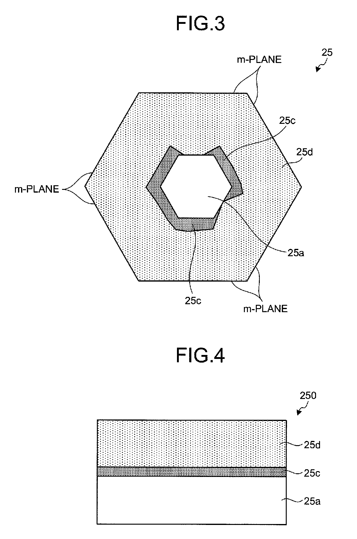
[0261]The seed crystal 27 manufactured in Seed Crystal Production Example 1 was used. This seed crystal 27 had a width of 1 mm and a length of about 40 mm. In the seed crystal 27 used in this Example, the fourth region 25b covered the entire outer circumference of the first region 25a in at least part of a c-plane cross section, in a manner similar to that shown in FIG. 5. In the c-plane cross section of the seed crystal 27, the thickness t (the thickness in an m-axis direction) of the fourth region 25b was found to be at least 10 μm.
[0262]First, the inner vessel 51 was separated from the crystal manufacturing apparatus 2 at the valve 61 and placed in a glove box with an Ar atmosphere. Then the seed crystal 27 was placed in an alumina-made reactor vessel 52 having an ...
example a2
[0268]In this Example, a crystal was grown in the crystal manufacturing apparatus 2 shown in FIG. 11 under the same conditions as in Example A1 except that the seed crystal 27 manufactured in Seed Crystal Production Example 2 above was used as a seed crystal, so that a group 13 nitride crystal was manufactured as an example of the group 13 nitride crystal 251.
[0269]As in the group 13 nitride crystal obtained in Example A1, the group 13 nitride crystal obtained in Example A2 had a hexagonal pyramid-shaped upper portion and a hexagonal columnar lower portion.
—Evaluation—
[0270]Photoluminescence (PL) from each of the group 13 nitride crystals manufactured in Examples A1 and A2 above was measured at room temperature under the same conditions as those in the measurement for the seed crystals.
[0271]The photoluminescence was measured for each of the first region 25a, the second region 25c, and the third region 25d.
[0272]The results showed that, in each of the group 13 nitride crystals manu...
PUM
| Property | Measurement | Unit |
|---|---|---|
| diameter | aaaaa | aaaaa |
| diameter | aaaaa | aaaaa |
| pressure | aaaaa | aaaaa |
Abstract
Description
Claims
Application Information
 - R&D
- Intellectual Property
- Life Sciences
- Materials
- Tech Scout
- Unparalleled Data Quality
- Higher Quality Content
- 60% Fewer Hallucinations
Browse by: Latest US Patents, China's latest patents, Technical Efficacy Thesaurus, Application Domain, Technology Topic, Popular Technical Reports.
© 2025 PatSnap. All rights reserved.Legal|Privacy policy|Modern Slavery Act Transparency Statement|Sitemap|About US| Contact US: help@patsnap.com