
Method for fabricating glass substrate package

a technology of glass substrate and packaging, which is applied in the direction of final product manufacturing, sustainable manufacturing/processing, fixed capacitors, etc., can solve the problems of increasing the negative impact of circuit performance, significantly degrading the chip performance, and increasing the capacitance of these wires

Inactive Publication Date: 2017-04-04
YANG PING JUNG
View PDF56 Cites 11 Cited by
  • Summary
  • Abstract
  • Description
  • Claims
  • Application Information

AI Technical Summary

Problems solved by technology

The metal connections which connect the Integrated Circuit to other circuit or system components become of relative more importance and have, with the further miniaturization of the IC, an increasingly negative impact on the circuit performance.
The parasitic capacitance and resistance of the metal interconnections increase, which degrades the chip performance significantly.
Attempts to reduce the resistance by using wider metal lines result in higher capacitance of these wires.
However, pre-testability, post-bonding visual inspection, and TCE (Temperature Coefficient of Expansion) matching to avoid solder bump fatigue are still challenges.
Glass has some disadvantages in comparison to silicon—notably its lower thermal conductivity and the difficulty in forming Through Glass Vias (TGV's).

Method used


Image

  • Method for fabricating glass substrate package
  • Method for fabricating glass substrate package
  • Method for fabricating glass substrate package

Examples


Embodiment Construction

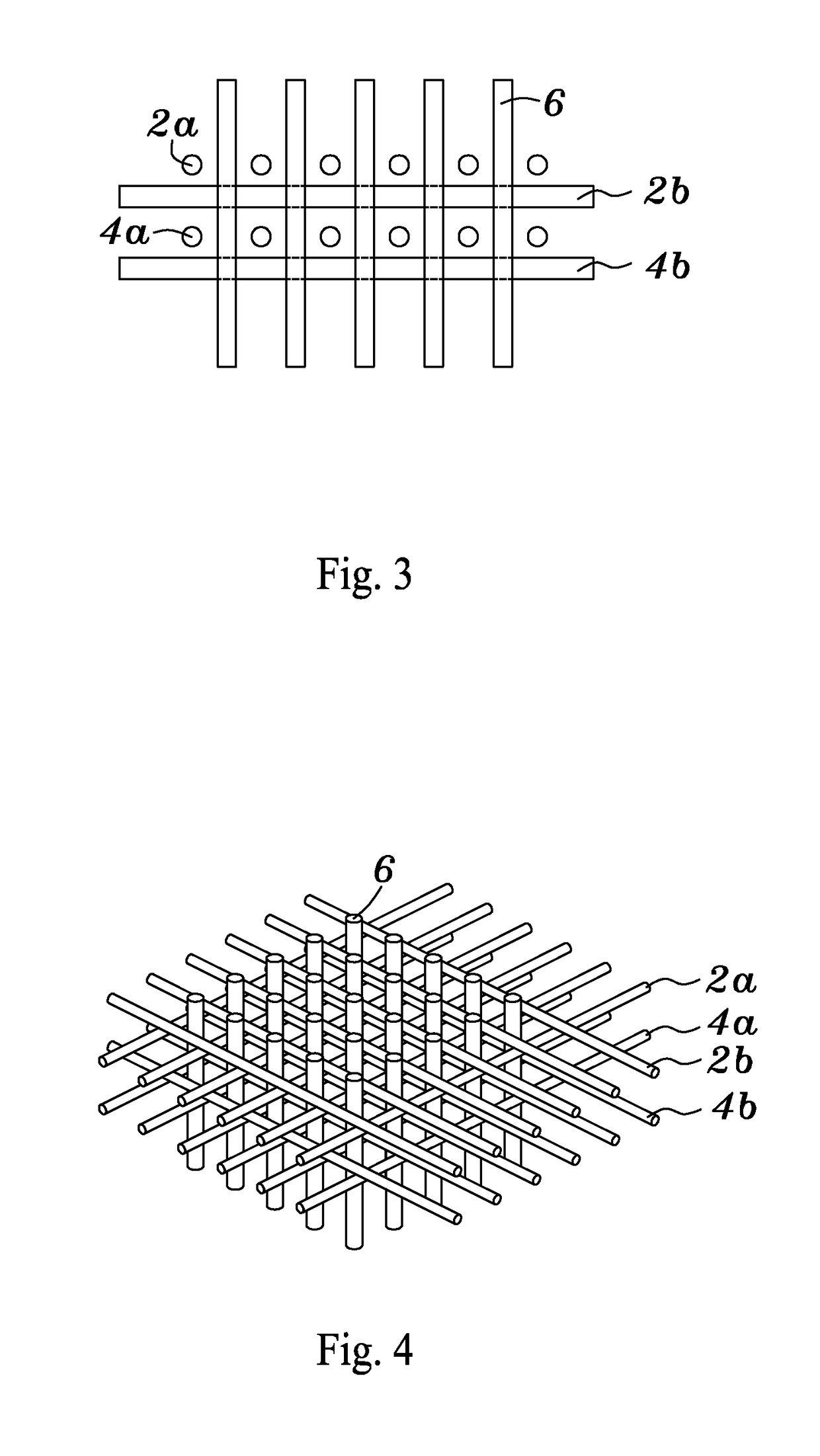
[0036]FIG. 1 illustrates a three-dimensional view of a net 2, 4, wherein the net 4 is under the net 2, wherein the net 2 comprises multiple Y-axis traces 2a and multiple X-axis traces 2b under the Y-axis traces 2a, and wherein the net 4 comprises multiple Y-axis traces 4a and multiple X-axis traces 4b under the Y-axis traces 4a. Multiple gaps 3, 5 form in the net 2 and 4. Each of the traces 2a, 2b, 4a and 4b is easily move to change the size of gaps 3 and gaps 5. The diameter (or width) of traces 2a, 2b, 4a and 4b are the same, such as between 10 and 30 micrometers, between 20 and 100 micrometers, between 40 and 150 micrometers, between 50 and 200 micrometers, between 200 and 1000 micrometers or between 500 and 10000 micrometers. The traces 2a, 2b, 4a and 4b may be metal traces or polymer traces, such as copper traces, copper-gold alloy traces, copper-gold-palladium alloy traces, copper-gold-silver alloy traces, copper-platinum alloy traces, copper-iron alloy traces, copper-nickel a...


PUM

PropertyMeasurementUnit
glass transition temperatureaaaaaaaaaa
widthaaaaaaaaaa

Abstract

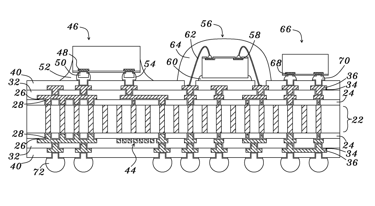
A substrate comprising a solid glass core having a first surface and a second surface opposed to the first surface; multiple conductors extending through the solid glass core beginning at the first surface and ending at the second surface, wherein one of the conductors has a third surface and a fourth surface, wherein the third surface and the first surface are substantially coplanar, wherein the second surface and the fourth surface are substantially coplanar, wherein one of the conductors comprise a copper-tungsten alloy material, wherein the solid glass core is directly contact with the conductor; and a first dielectric layer and a first metal layer formed at the first surface, wherein the first metal layer at the first surface is electrically coupled with one of the conductors.

Description

CROSS-REFERENCE TO RELATED APPLICATIONS[0001]This application claims the benefit of priority from U.S. Provisional Patent Application Ser. No. 61 / 705,649, entitled “METHOD FOR FABRICATING GLASS SUBSTRATE PACKAGE,” filed on Sep. 26, 2012, which is herein incorporated by reference in its entirety.BACKGROUND OF THE DISCLOSURE[0002]Field of the Disclosure[0003]The patent disclosure a method and structure to manufacture a glass substrate, and disclosed embodiments relate to one or more chip building a system on the glass substrate.[0004]Brief Description of the Related Art[0005]As is well known, microelectronic devices have a tendency to be minimized and thinned with its functional development and a semiconductor package mounted on a mother board is also following the tendency in order to realize a mounting of high integration.[0006]When the geometric dimensions of the Integrated Circuits are scaled down, the cost per die is decreased while some aspects of performance are improved. The m...

Claims


Application Information

Patent Timeline
Patent Type & Authority Patents(United States)
IPC IPC(8): H05K1/09H01L23/15H01L23/49H01L51/00H01L23/498H01L23/00H01L25/16H05B44/00
CPCH05K1/09H01L23/15H01L23/49811H01L23/49827H01L23/49833H01L51/0096H01L24/13H01L24/16H01L25/16H01L2224/0401H01L2224/05124H01L2224/05147H01L2224/05599H01L2224/131H01L2224/1308H01L2224/13076H01L2224/13111H01L2224/13144H01L2224/13147H01L2224/13155H01L2224/16145H01L2224/16225H01L2224/16237H01L2224/2919H01L2224/32225H01L2224/45144H01L2224/45147H01L2224/48091H01L2224/48228H01L2224/48465H01L2224/73204H01L2224/73265H01L2924/12042H01L2924/12044H01L2924/1461H01L2924/15311H01L2924/181H01L2924/30107Y02E10/549H01L2924/00014H01L2224/48227H01L2924/00H01L2924/014H01L2924/00012H01L2224/45124H01L2224/45139H01L24/48Y02P70/50H10K77/10H01L2924/01029H05B45/60H01G4/129H01L24/30H01L24/46H01L24/49H01L2224/056H01L2224/05688H01L2224/05788H01L2224/32151
Inventor YANG, PING-JUNG
Owner YANG PING JUNG
Learn More