Method for separating surface layer or growth layer of diamond

a growth layer and surface layer technology, applied in the direction of polycrystalline material growth, manufacturing tools, after-treatment details, etc., can solve the problems of reducing yield, synthesis requiring an extremely long time, and high cost of large single-crystal diamonds, so as to achieve easy separation, short separation time, and high separation efficiency

Active Publication Date: 2016-08-09
NAT INST OF ADVANCED IND SCI & TECH
View PDF8 Cites 0 Cited by
  • Summary
  • Abstract
  • Description
  • Claims
  • Application Information

AI Technical Summary

Benefits of technology

[0016]According to the method of the invention for separating a surface layer of a diamond, a single-crystal diamond or a polycrystal diamond, is used as a raw material, and a non-diamond layer is formed in the diamond, after which etching is performed by applying an alternating-current (AC) voltage, thereby allowing a surface portion of the diamond to be separated in a short period of time.
[0017]Further, a diamond is grown on a diamond seed crystal of a single-crystal diamond or a polycrystal diamond by a vapor-phase synthesis method, after which the above-described etching method is applied, thereby allowing the diamond film grown on the seed crystal to be separated in a short period of time. In this way, even a large single-crystal diamond substrate exceeding 5×5 mm in size can be produced easily in a short period of time. According to this method, the seed crystal used in the production of a diamond or the resulting diamond substrate can be reused as a seed crystal. Thus, the number of substrates produced can be dramatically increased, enabling production of substrates at low cost and in large quantities.

Problems solved by technology

On the other hand, single-crystal diamond substrates are obtained by slicing a natural or synthetic single-crystal diamond by a method such as cleavage, sawing, laser cutting, or the like, and polishing the diamond, as required; however, large single-crystal diamonds are very expensive when they are natural.
Further, when single-crystal diamonds are produced according to a high-temperature high-pressure synthesis method, the synthesis requires an extremely long time, and the yield decreases as the crystal size increases.
In this case, because the large crystal used as a seed is expensive and valuable, separation of the large single-crystal substrate from the vapor-phase synthetic diamond in a reusable form is strongly desired.
However, as etching proceeds farther inside, the supply of oxygen that passes through the etched non-diamond layer decreases, thereby reducing the etching rate.
However, because the ion dose increases, the surface layer of the diamond is damaged by radiation.
Even in this case, however, as the substrate size increases, the etching rate inside the crystal decreases, thus requiring a very long period of time for etching.
For this reason, the size of the diamond used is limited to from 2.5×2.5 mm to 4×4 mm, and application to substrates with a size exceeding this range is practically difficult.
This method also has the above-mentioned problem of electrochemical etching.

Method used


Image

  • Method for separating surface layer or growth layer of diamond
  • Method for separating surface layer or growth layer of diamond

Examples


example 1

[0061]A high-temperature high-pressure synthetic Ib diamond (100) substrate with a size of 9.3×9.5×1.05 mm3 was used as a substrate, and carbon ions were implanted into the substrate at an implantation energy of 3 MeV and a dose of 2×10¹⁶ ions / cm2, using a 1.5 MV tandem accelerator. The projectile range of the implanted ions was calculated using a Monte Carlo simulation code, and the result was about 1.6 μm. As a result of this irradiation, the color of the diamond substrate changed from a pale yellow to black; this confirmed that a non-diamond layer had been formed.

[0062]The ion-implanted substrate was placed in a commercially available microwave plasma CVD apparatus, after which hydrogen gas was introduced into the CVD chamber, and microwave power was applied to generate plasma. The microwave power was set to about 3 kW, with the hydrogen gas flow rate set at 500 sccm and the pressure at 24 kPa, so that the substrate temperature was 1,130° C., and these conditions were maintained ...

example 2

[0067]A diamond was produced by growing a vapor-phase synthetic diamond to a thickness of 8.7 mm on a high-temperature high-pressure synthetic Ib diamond (100) substrate with a size of about 6×6 mm according to a microwave plasma CVD method. The resulting bulk single crystal was sliced along the (100) plane perpendicular to the growth face, and the surface of the slice was polished to prepare a single-crystal diamond substrate in the form of a 6×8.5×1.02 mm3 trapezoid. Using this substrate, ion implantation and epitaxial growth of a diamond by a microwave plasma CVD method were performed according to the same method as Example 1.

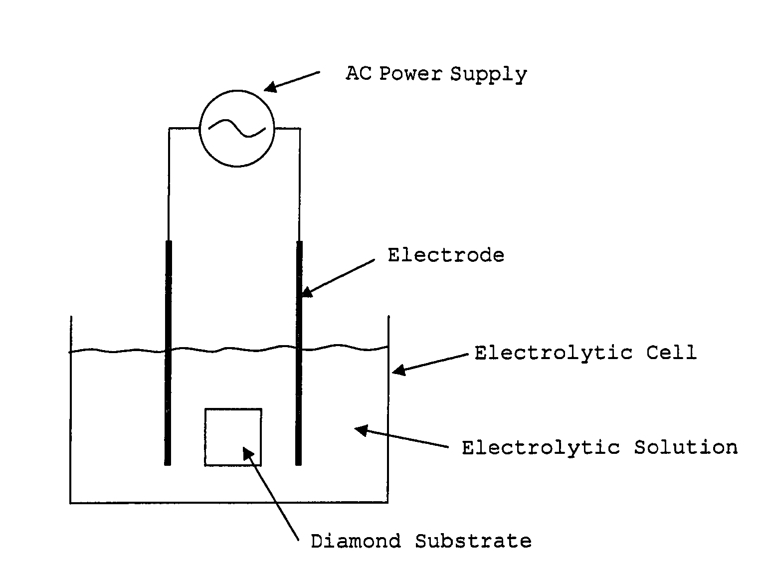
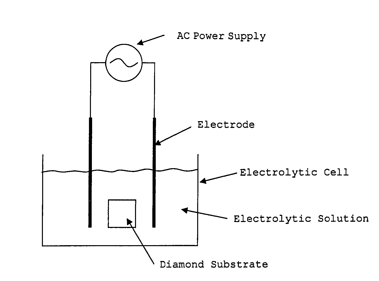
[0068]After the growth, the diamond deposited around the ion-implanted layer on the substrate-side surface was removed by laser cutting, and etching was performed in the same manner as Example 1. An AC voltage with an effective value of 5.6 kV and a frequency of 60 Hz was applied across the electrodes, using pure water as an electrolytic solution, with the e...

example 3

[0072]The surface (the separated face) of the high-temperature high-pressure synthetic Ib diamond (100) substrate, i.e., the surface from which the diamond grown layer was separated in Example 1, was subjected to ion implantation and diamond growth by a microwave CVD method according to the same method as Example 1.

[0073]After the growth of a single-crystal diamond, the diamond deposited around the ion-implanted layer on the substrate-side surface was removed by laser cutting, and etching was performed by applying an AC voltage in pure water as in Example 1, thereby separating the diamond grown layer from the substrate. As a result, a CVD diamond plate with a thickness of about 400 μm was separated.

[0074]As a result of repeating this method three times, CVD diamond plates of similar thicknesses were successfully separated.


PUM

PropertyMeasurementUnit
resistivityaaaaaaaaaa
sizeaaaaaaaaaa
sizeaaaaaaaaaa

Abstract

The present invention provides a method for separating a surface layer of a diamond, which comprises implanting ions into a diamond to form a non-diamond layer near a surface of the diamond; and etching the non-diamond layer in the diamond by applying an alternating-current voltage across electrodes in an electrolytic solution; and a method for separating a grown layer of a diamond, which further comprises the step of growing a diamond by a vapor-phase synthesis method, after forming a non-diamond layer according to the above-described method. The invention is applicable to various single-crystal and polycrystal diamonds. More specifically, even with a large single-crystal diamond, a portion of the single-crystal diamond can be efficiently separated in a reusable form in a relatively short period of time.

Description

TECHNICAL FIELD[0001]The present invention relates to a method for separating a surface layer or a growth layer of a diamond, such as a single-crystal diamond, a polycrystal diamond, or the like, which is widely used as tools, grindstones, substrates for electronic devices, etc.BACKGROUND ART[0002]Diamond is widely used as tools, grindstones, substrates for electronic devices, etc.[0003]For all of these uses, the realization of large diamond substrates is desired. With polycrystal diamond substrates, large substrates exceeding 2 inches in size are already being produced. On the other hand, single-crystal diamond substrates are obtained by slicing a natural or synthetic single-crystal diamond by a method such as cleavage, sawing, laser cutting, or the like, and polishing the diamond, as required; however, large single-crystal diamonds are very expensive when they are natural. Further, when single-crystal diamonds are produced according to a high-temperature high-pressure synthesis me...

Claims


Application Information

Patent Timeline
Patent Type & Authority Patents(United States)
IPC IPC(8): C23C16/01C23C16/27C23C16/56C25F3/00C30B29/04C30B31/22C30B33/06
CPCC23C16/01C23C16/27C23C16/56C25F3/00C30B29/04C30B31/22C30B33/06
Inventor MOKUNO, YOSHIAKICHAYAHARA, AKIYOSHIYAMADA, HIDEAKI
Owner NAT INST OF ADVANCED IND SCI & TECH
Why Eureka
Try Eureka