Avalanche photodiode semiconductor structure having a high signal-to-noise ratio and method for manufacturing such a photodiode

a photodiode and semiconductor technology, applied in the direction of semiconductor devices, basic electric elements, electrical appliances, etc., can solve the problem that the sensitivity of such a structure is still not sufficient for certain applications, and achieve the effect of substantial variation in the energy band gap

Active Publication Date: 2016-08-02
COMMISSARIAT A LENERGIE ATOMIQUE ET AUX ENERGIES ALTERNATIVES
View PDF8 Cites 5 Cited by
  • Summary
  • Abstract
  • Description
  • Claims
  • Application Information

AI Technical Summary

Benefits of technology

[0024]As such, the carriers generated in the first area, during their transit to the third area, pass in turn the first subpart and the second subpart. The first subpart, by having a reduced mean carrier multiplication rate by micrometer, makes it possible to increase the carrier current with a reduction in the signal-to-noise ratio that remains contained. The carrier current is as such slightly increased with a signal-to-noise ratio that remains substantial. The carrier current then transits by the second subpart wherein it is significantly increased by the strong mean carrier multiplication rate by micrometer that the second subpart has.
[0058]Such substeps make it possible to provide a structure with a second area that, while still having a multiplication of carriers by impact ionisation that is preponderant for the electrons with the second subpart which has an energy band gap greater than that of the first subpart, comprises an interface between the first and the second subpart substantially exempt of crystal defects. Indeed the mercury-cadmium tellurides allow for a substantial variation in the energy band gap by varying the proportion of cadmium without a significant variation in the parameters of the crystal lattice structure.

Problems solved by technology

Nevertheless, although this type of structure has an improved sensitivity with regards to an avalanche photodiode structure that does not comprise a second area suitable for providing a multiplication of carriers by impact ionisation that is preponderant for one type of carrier, the sensitivity of such a structure is still not sufficient for certain applications, such as detecting single photons at ambient temperature.

Method used


Image

  • Avalanche photodiode semiconductor structure having a high signal-to-noise ratio and method for manufacturing such a photodiode
  • Avalanche photodiode semiconductor structure having a high signal-to-noise ratio and method for manufacturing such a photodiode
  • Avalanche photodiode semiconductor structure having a high signal-to-noise ratio and method for manufacturing such a photodiode

Examples


first embodiment

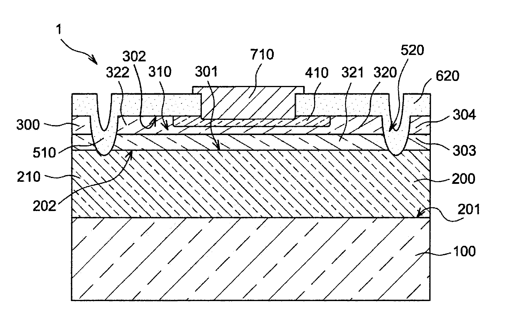
[0067]FIG. 1 shows a semiconductor structure 1 said structure 1 being intended for the detecting and measuring of an electromagnetic radiation of which the wavelength is included in a given wavelength range.

[0068]In order to show and facilitate the understanding of the operation of the structure according to the invention, the values and the materials which are mentioned hereinbelow, when this is stated, relate to a particular application of the invention for the detecting and measuring of electromagnetic radiation of which the wavelength is included in the near-infrared wavelength range. Of course, the values and the materials relating to this application are provided solely for the purposes of information and are not restrictive.

[0069]It is meant hereinabove and in the rest of this document by near-infrared wavelength range a wavelength range between 0.8 μm and 3 μm.

[0070]A structure 1 according to the first embodiment of the invention comprises:[0071]a support 100,[0072]a first ...
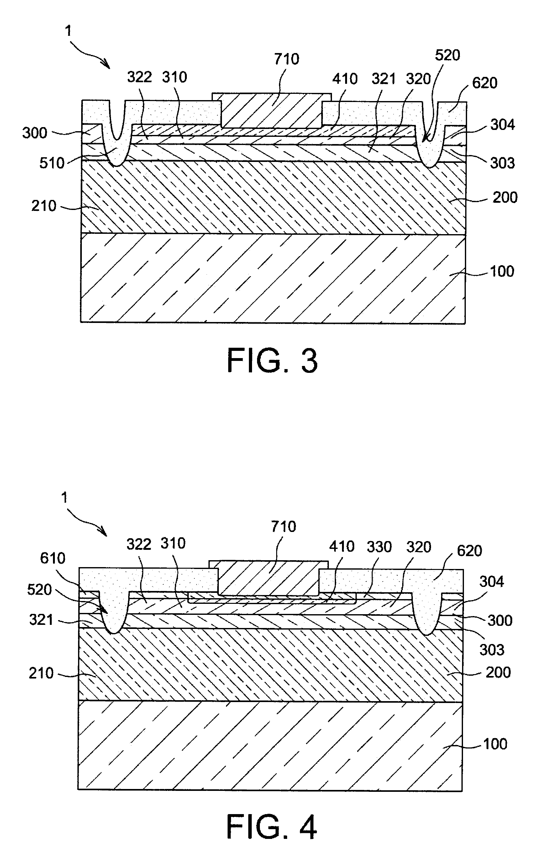
third embodiment

[0137]In this third embodiment, the second semiconductor layer 300 comprises a second face 302 which is opposite the first face. The second layer 300 is in contact via its second face 302 with the adaptation layer 610.

[0138]The adaptation layer 610 is a third semiconductor layer which is adapted for forming a good interface between the second semiconductor layer 300 and the passivation layer 620. To this effect, the adaptation layer 610 has an intermediate an energy band gap between that of the major part 320 of the second area 310 and the energy band gap of the passivation layer 620.

[0139]The adaptation layer 610 is of the second type of conductivity. The adaptation layer 610 comprises, excluding its part forming the third area 410, a majority carrier d s which is of the same order of magnitude as that of the major part 320 of the second area 310 and preferentially substantially equal to that of the major part 320 of the second area 310. As such the adaptation layer 610 comprises a...


PUM


Abstract

A semiconductor structure, and method for manufacturing, of avalanche photodiode type for receiving electromagnetic radiation in a given wavelength range and including a first semiconductor area configured for absorption of the electromagnetic radiation, a second area configured for providing a multiplication of carriers, and a third semiconductor area in contact with the second semiconductor area. The second area includes at least two subparts with the second subpart configured to have a mean carrier multiplication rate that is more substantial than that of the first subpart.

Description

TECHNICAL FIELD[0001]The invention relates to the field of devices for measuring and detecting light.[0002]In the last few years, the application of methods for manufacturing microelectronics to direct gap semiconductor materials have made it possible to improve the performance of optoelectronic structures.[0003]Among these optoelectronic structures, avalanche photodiodes have improved sensitivity with a sharp drop in dark current. Nevertheless, despite the improvement in this sensitivity, detecting single photons at ambient temperature still remains difficult with such structures.[0004]As such, the improvement in the sensitivity of avalanche photodiodes remains a current problem.[0005]The invention therefore relates more particularly to an avalanche photodiode semiconductor structure having a high signal-to-noise ratio and to a method for manufacturing such a structure.PRIOR ART[0006]In the last few years, various avenues for research have been explored in order to improve avalanch...

Claims


Application Information

Patent Timeline
Patent Type & Authority Patents(United States)
IPC IPC(8): H01L31/10H01L31/107H01L31/0296H01L31/18
CPCH01L31/1075H01L31/02966H01L31/1832
Inventor ROTHMAN, JOHAN
Owner COMMISSARIAT A LENERGIE ATOMIQUE ET AUX ENERGIES ALTERNATIVES
Why Eureka
Try Eureka