
Method for manufacturing high-strength structural stacked capacitor

a technology of structural stacked capacitors and capacitors, which is applied in the direction of capacitors, semiconductor devices, electrical apparatus, etc., can solve problems such as weakening structural strength, and achieve the effects of increasing capacitance, improving structural strength of electrodes, and increasing electrodes

Active Publication Date: 2016-05-24
MICRON TECH INC
View PDF5 Cites 2 Cited by
  • Summary
  • Abstract
  • Description
  • Claims
  • Application Information

AI Technical Summary

Benefits of technology

[0007]The object of the instant disclosure is to provide a method for manufacturing high-strength structural stacked capacitor which can overcome limitations of the traditional one. Moreover, double-side capacitors manufactured by the method have larger electrode contact-surface area can be allowed to increase capacitance as well as to ensure that the structural strength of the electrode structure has been improved to prevent the lower electrode from toppling in wet-etching.
[0009]Base on above, the method begins to form a part of upper electrode layer to cover a first surface of each of the lower electrode layers before a wet etching process. After that, another part of upper electrode layer is formed to cover a second surface of each the lower electrode layers after the wet etching process. Therefore, the high-strength structural lower electrode can be achieved during overall process to improve production yield.

Problems solved by technology

In summary, the increased height or the decreased thickness of the capacitor electrode will result in weakening the structural strength then twin bit failure occurs.

Method used


Image

  • Method for manufacturing high-strength structural stacked capacitor
  • Method for manufacturing high-strength structural stacked capacitor
  • Method for manufacturing high-strength structural stacked capacitor

Examples


Embodiment Construction

[0014]The aforementioned illustrations and following detailed descriptions are exemplary for the purpose of further explaining the scope of the instant disclosure. Other objectives and advantages related to the instant disclosure will be illustrated in the subsequent descriptions and appended drawings.

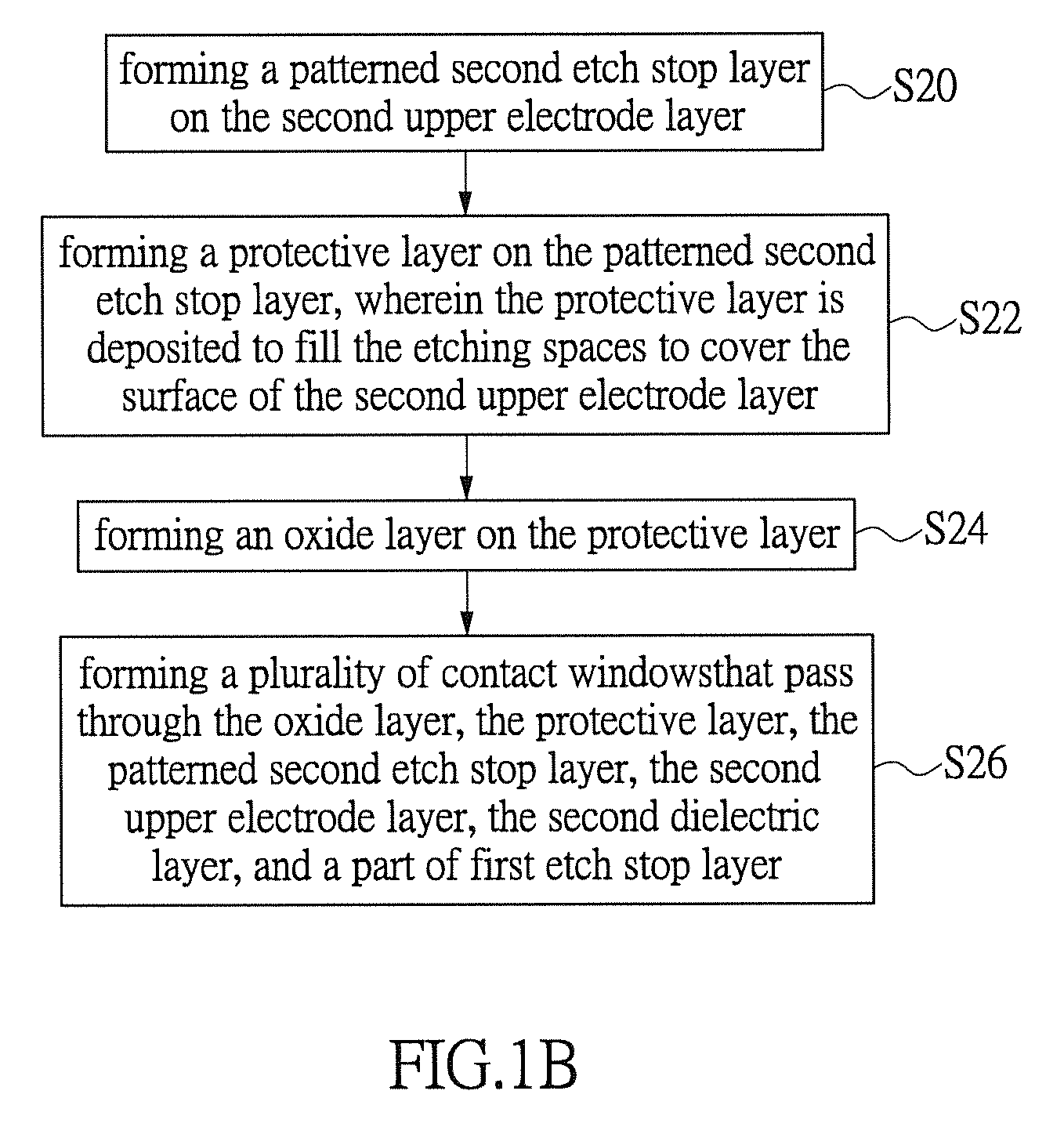
[0015]Please refer to FIG. 1A as well as FIGS. 2 to 7. FIG. 1A is a process diagram of a method for manufacturing high-strength structural stacked capacitor according to a preferred embodiment of the instant disclosure. FIGS. 2 to 7 are cross-sectional views illustrating the processing steps of the method. Basically, the method of the instant disclosure has the following steps:

[0016]Step S10 is providing a substrate 100, and then forming a laminate structure 110 having a sacrificial layer 114 on a substrate 100. Referring to FIG. 2, the substrate 100, in practice, can be a silicon substrate or any other suitable substrate having a plurality of contact plugs 102 formed therein. Moreover...


PUM

PropertyMeasurementUnit
strengthaaaaaaaaaa
areaaaaaaaaaaa
memory capacitanceaaaaaaaaaa

Abstract

The instant disclosure relates to a method for manufacturing high-strength structural stacked capacitor. The novel feature of the instant disclosure is forming a part of upper electrode layer to cover the first / outer surface of each of the lower electrode layers before removing the sacrificial layer, and forming another part of upper electrode layer to cover the second / inner surface of each of the lower electrode layers after removing the sacrificial layer. Hence, the structure strength of the lower electrode layer in all process steps has been improved.

Description

BACKGROUND OF THE INVENTION[0001]1. Field of the Invention[0002]The instant disclosure relates to a semiconductor manufacturing technology; in particular, to a method for manufacturing high-strength structural stacked capacitor.[0003]2. Description of Related Art[0004]Dynamic random access memory (DRAM) is one kind of widely used integrated circuit element. With the vigorous development of semiconductor industry, the dimension of integrated circuit elements nowadays range from micron size to submicron size. For DRAM, that is to say, the cross-sectional area of each capacitor and each gap between capacitors become smaller. Basically, the better operating capability of computer software becomes, the greater memory capacitance of computer hardware need. Facing up to the problem of the capacitor dimension become smaller, but the memory capacitance must be increased. The traditional method of manufacturing DRAM capacitors certainly needs to be improved.[0005]Generally, the following meth...

Claims


Application Information

Patent Timeline
Patent Type & Authority Patents(United States)
IPC IPC(8): H01L21/20H01L21/768H01L27/108H01L49/02
CPCH01L27/10814H01L21/7682H01L27/10817H01L27/10855H01L28/91H01L21/02H10B12/30H10B12/37H10B12/315H10B12/318H10B12/0335
Inventor HUNG, HAI-HANLIN, YI-REN
Owner MICRON TECH INC
Learn More