Silicon carbide semiconductor device

a technology of silicon carbide and semiconductors, applied in the direction of semiconductor devices, basic electric elements, electrical appliances, etc., can solve the problems of increased leak current, increased loss of energization, and schottky barrier diodes, etc., and achieve the effect of sufficient breakdown voltag

Active Publication Date: 2015-11-10
MITSUBISHI ELECTRIC CORP
View PDF21 Cites 0 Cited by
  • Summary
  • Abstract
  • Description
  • Claims
  • Application Information

AI Technical Summary

Benefits of technology

[0012]It is an object of the present invention to provide a silicon carbide semiconductor device in which a sufficient breakdown voltage can be achieved with less number of ion implantations.
[0014]According to the above aspect of the present invention, since the second conductivity type region is formed of a plurality of unit cells arranged therein, each of which is a repeating unit of a distribution of a second conductivity type impurity, and each of the unit cells has at least a first distribution region in which the second conductivity type impurity is distributed at first concentration and a second distribution region in which the second conductivity type impurity is distributed at second concentration higher than the first concentration, it is possible to adjust a concentration distribution of the second conductivity type impurity by combination of the first distribution region and the second distribution region even with less number of ion implantations. Further, with such an arrangement of the plurality of unit cells, since the second conductivity type impurity is not locally distributed, it is also possible to achieve a sufficient breakdown voltage.

Problems solved by technology

The Schottky barrier diode (SBD) has problems of an increase in the leak current in application of reverse bias and an increase in a loss in energization in a case where it is intended to achieve high breakdown voltage.
Therefore, there arises a problem of an increase in the number of ion implantation processes.
Further, since the P-type regions are locally formed, surge current is concentrated and this arises a problem that high breakdown voltage cannot be achieved.

Method used


Image

  • Silicon carbide semiconductor device
  • Silicon carbide semiconductor device
  • Silicon carbide semiconductor device

Examples


Embodiment Construction

[0028]Hereinafter, with reference to figures, discussion will be made on the preferred embodiment of the present invention.

[0029]

[0030]

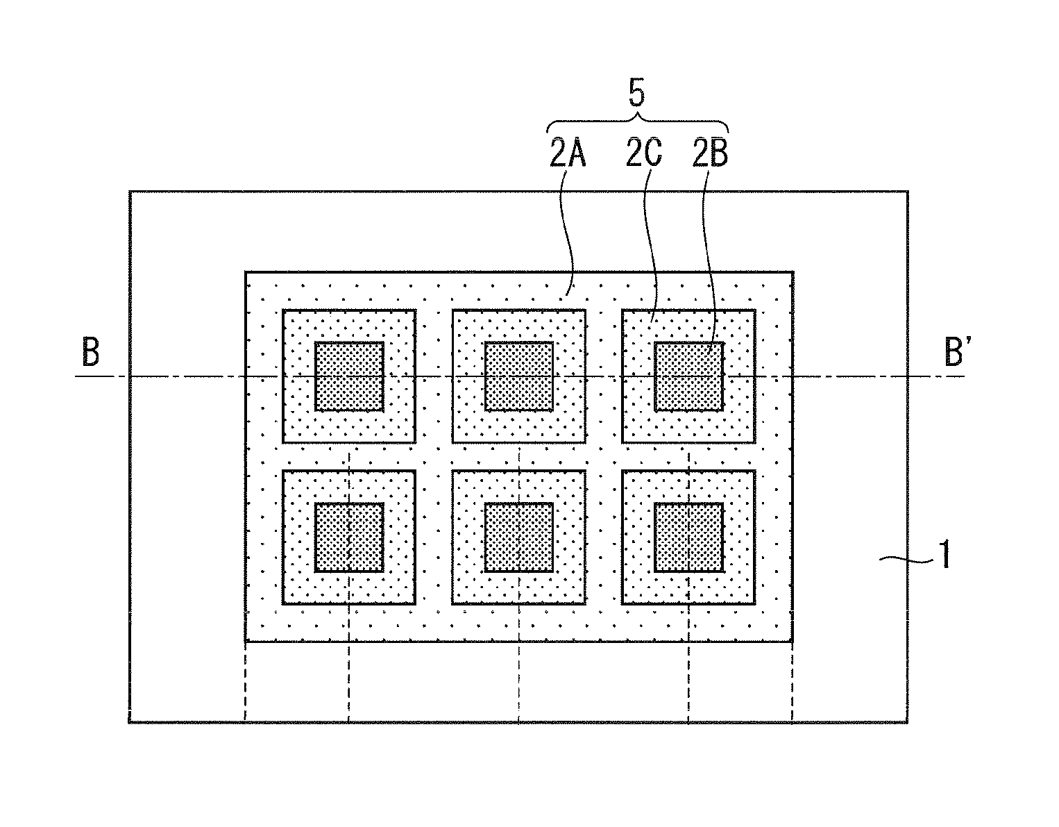
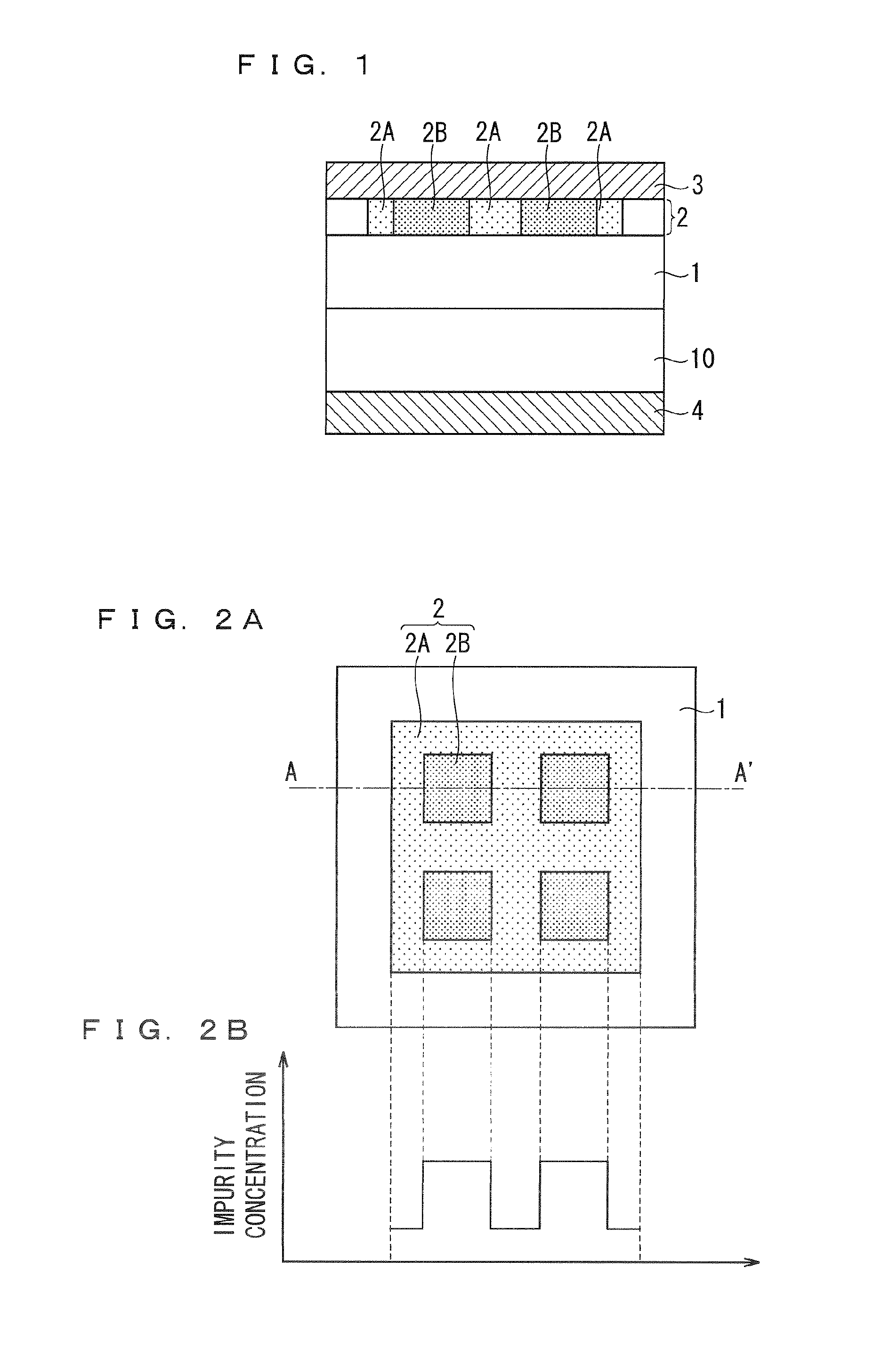
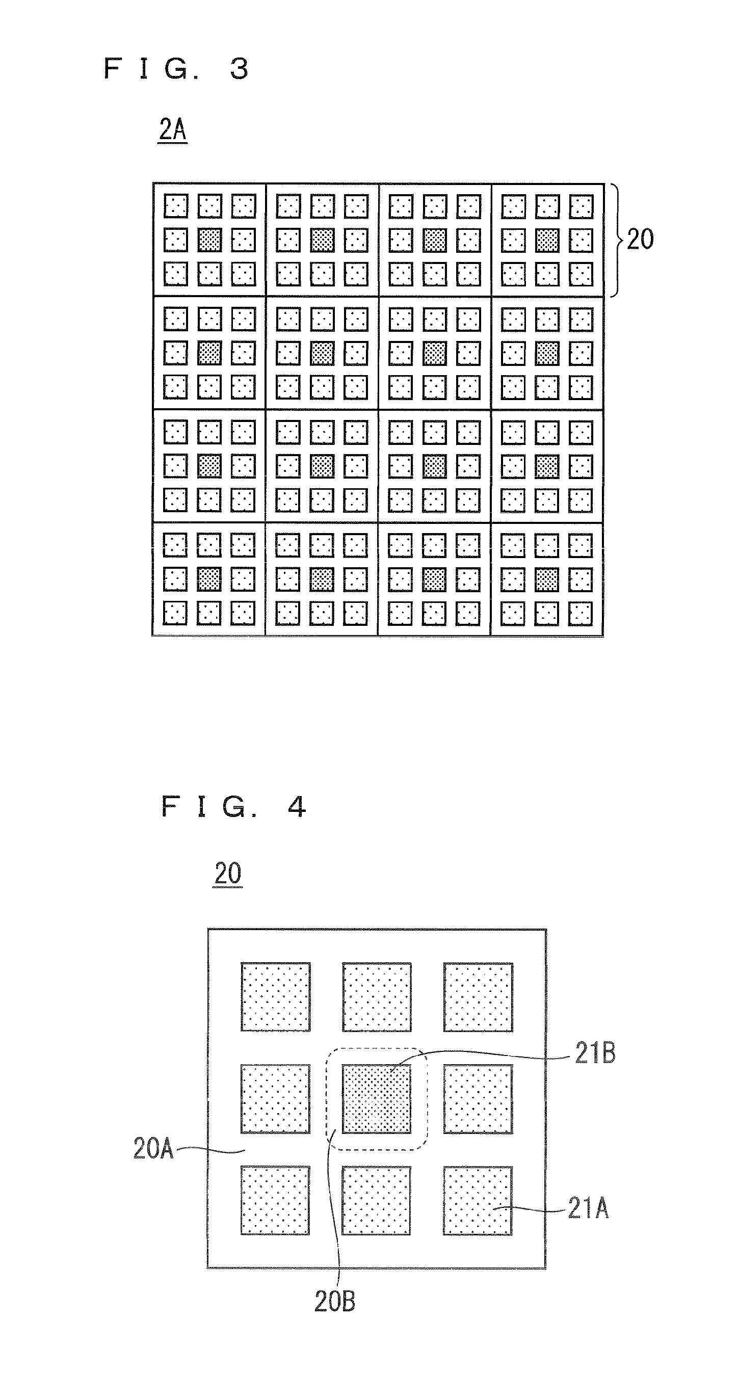
[0031]FIG. 1 is a cross section showing a structure of a silicon carbide semiconductor device in accordance with the preferred embodiment of the present invention. Though a JBS or an MPS using silicon carbide will be shown as an example in this preferred embodiment, the silicon carbide semiconductor device of the present invention is not limited to these structures but may be an SBD, a MOSFET, or the like.

[0032]As shown in FIG. 1, the silicon carbide semiconductor device comprises an N−, -type (first conductivity type) silicon carbide drift layer 1 formed on an N+, -type (first conductivity type) silicon carbide substrate 10 by epitaxial growth, a P-type region 2 which is a second conductivity type region formed in a surface layer of the silicon carbide drift layer 1, a Schottky electrode 3 formed above the silicon carbide drift layer 1 corresponding...


PUM

PropertyMeasurementUnit
currentaaaaaaaaaa
conductivity typeaaaaaaaaaa
conductivityaaaaaaaaaa

Abstract

A silicon carbide semiconductor device of the present invention comprises a silicon carbide drift layer formed on a silicon carbide substrate, a P-type region formed in a surface layer of the silicon carbide drift layer, and a Schottky electrode formed above the silicon carbide drift layer correspondingly to a forming portion of the P-type region. The P-type region is formed of a plurality of unit cells arranged therein. Each of the unit cells has at least a first distribution region in which the P-type impurity is distributed at first concentration and a second distribution region in which the P-type impurity is distributed at second concentration higher than the first concentration. With this structure, it is possible to provide a silicon carbide semiconductor device in which a sufficient breakdown voltage can be achieved with less number of ion implantations.

Description

BACKGROUND OF THE INVENTION[0001]1. Field of the Invention[0002]The present invention relates to a silicon carbide semiconductor device, and more particularly to a JBS (Junction Barrier controlled Schottky diode) or an MPS (Merged P-i-N / Schottky diode) which uses silicon carbide.[0003]2. Description of the Background Art[0004]The dielectric breakdown electric field of silicon carbide is about ten times as large as that of silicon and the band gap of silicon carbide is about three times as wide as that of silicon. Therefore, a power device using silicon carbide has a characteristic feature that allows a high temperature operation with low resistance as compared with a currently-used power device using silicon.[0005]Particularly, an SBD (Schottky Barrier Diode) and a MOSFET (Metal-Oxide-Semiconductor Field-Effect Transistor) which use silicon carbide can reduce a loss in an operation as compared at the same breakdown voltage with a pn diode and an IGBT (Insulated Gate Bipolar Transist...

Claims


Application Information

Patent Timeline
Patent Type & Authority Patents(United States)
IPC IPC(8): H01L29/15H01L31/0312H01L29/872H01L29/36H01L29/16H01L29/06
CPCH01L29/872H01L29/0619H01L29/36H01L29/0692H01L29/1608
Inventor KITANI, TAKESHITARUI, YOICHIRO
Owner MITSUBISHI ELECTRIC CORP
Why Eureka
Try Eureka