Process for producing a receiver substrate for a semiconductor-on-insulator structure for radiofrequency applications and process for producing such a structure

a technology of semiconductor on-insulator and receiver substrate, which is applied in the direction of semiconductor/solid-state device manufacturing, basic electric elements, electric apparatus, etc., can solve the problems of direct bonding process drawback, increase in production cost, and oxide layer located on the donor substrate, so as to achieve the effect of limiting production cos

Pending Publication Date: 2021-12-30
S O I TEC SILICON ON INSULATOR THECHNOLOGIES
View PDF1 Cites 0 Cited by
  • Summary
  • Abstract
  • Description
  • Claims
  • Application Information

AI Technical Summary

Benefits of technology

[0025]One aim of the present disclosure is to provide a process allowing the aforementioned drawbacks to be overcome. The present disclosure aims to provide such a process allowing a receiver substrate to be fabricated for a semiconductor-on-insulator structure the buried oxide layer of which possesses a sufficient breakdown voltage for radiofrequency applications, while limiting production cost.

Problems solved by technology

The direct-bonding process has the drawback that the oxide layer is located on the donor substrate.
Now, the higher the implantation energy, the larger the amount of ions to be implanted must be, and the lower the implantation current (current density), this leading to an increase in production cost, limiting the feasibility of the process, and, in particular, limiting the maximum thickness of the oxide layer.
In addition, this process decreases the reusability of the donor substrate, since some of the donor substrate is consumed to form the oxide layer.
The breakdown voltage is too low to be compatible with radiofrequency applications.
Fabrication of a substrate by reverse bonding therefore induces a drop in the maximum electric field, this resulting in a corresponding drop in breakdown voltage.

Method used


Image

  • Process for producing a receiver substrate for a semiconductor-on-insulator structure for radiofrequency applications and process for producing such a structure
  • Process for producing a receiver substrate for a semiconductor-on-insulator structure for radiofrequency applications and process for producing such a structure
  • Process for producing a receiver substrate for a semiconductor-on-insulator structure for radiofrequency applications and process for producing such a structure

Examples


Embodiment Construction

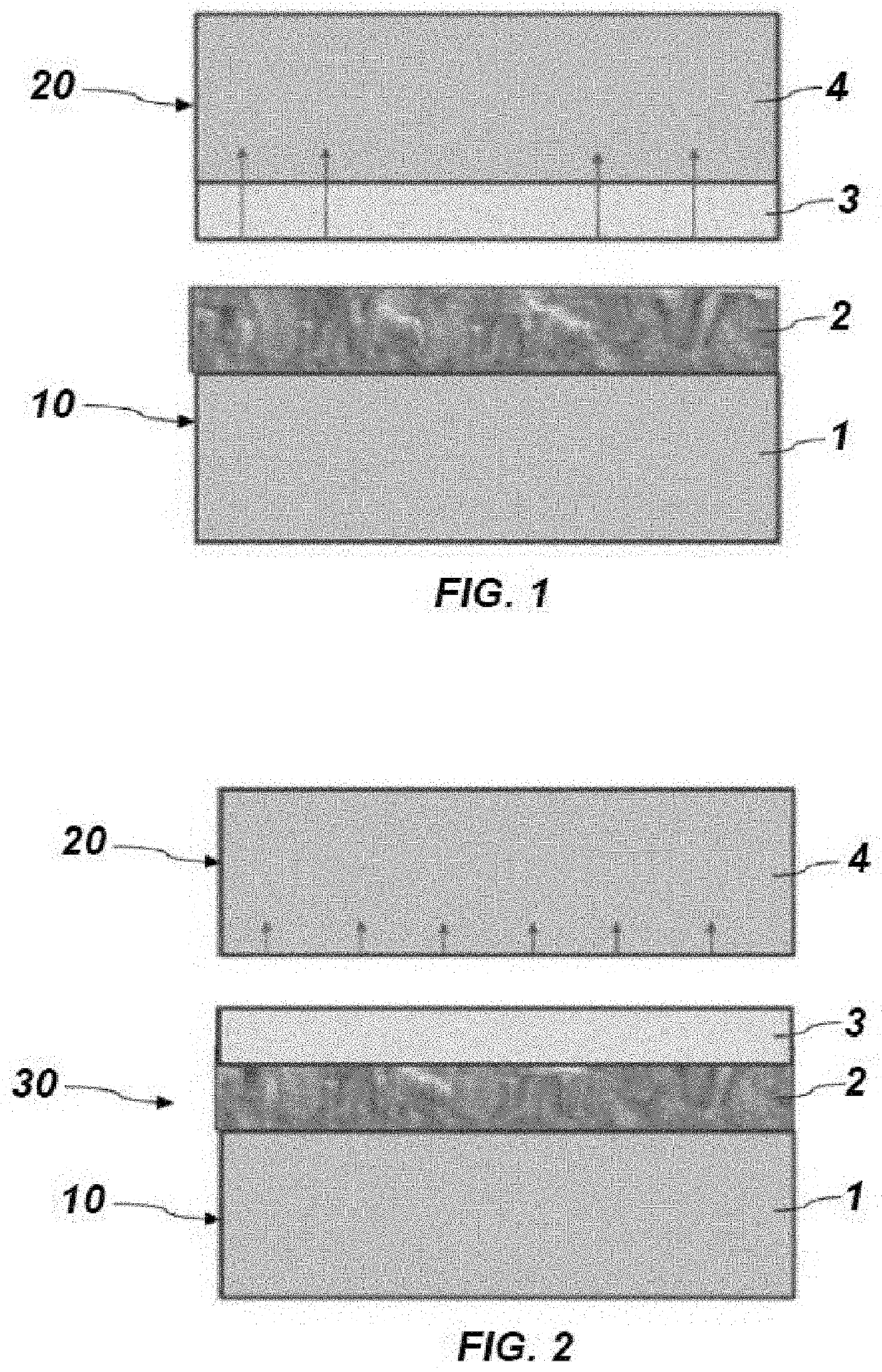
[0066]The present disclosure relates to a process for fabricating a receiver substrate (30) for a semiconductor-on-insulator structure for radiofrequency applications, comprising the following steps:

[0067]The process according to the present disclosure is a reverse-bonding process. It comprises, with reference to FIG. 2, a step of providing a semiconductor substrate 10 comprising a base substrate 1 made of single-crystal material and a charge-trapping layer 2 made of polysilicon arranged on the base substrate, followed by a step of oxidizing the charge-trapping layer 2 to form an oxide layer 3 arranged on the charge-trapping layer.

[0068]The charge-trapping layer 2 may be formed by epitaxy on the base substrate 1, or alternatively deposited on the base substrate, in particular, by chemical vapor deposition (CVD).

[0069]The charge-trapping layer 2 is oxidized at least partially at a temperature between 750° C. and 875° C.

[0070]Such a process makes it possible to form, by reverse bondin...


PUM

PropertyMeasurementUnit
temperatureaaaaaaaaaa

Abstract

A process for producing a receiver substrate for a semiconductor-on-insulator structure for radiofrequency application comprises the following steps: providing a semiconductor substrate comprising a base substrate made of monocrystalline material and a charge-trapping layer made of polycrystalline silicon arranged on the base substrate; oxidizing the charge-trapping layer to form an oxide layer arranged on the charge-trapping layer. The oxidation of the charge-trapping layer is performed at least partly at a temperature lower than or equal to 875° C., in the following manner: starting the oxidization at a first temperature (T1) between 750° C. and 1000° C.; decreasing the temperature down to a second temperature (T2), lower than the first temperature (T1), between 750° C. and 875° C.; continuing the oxidization at the second temperature (T2).

Description

CROSS-REFERENCE TO RELATED APPLICATIONS[0001]This application is a national phase entry under 35 U.S.C. § 371 of International Patent Application PCT / FR2020 / 050028, filed Jan. 8, 2020, designating the United States of America and published as International Patent Publication WO 2020 / 144438 A1 on Jul. 16, 2020, which claims the benefit under Article 8 of the Patent Cooperation Treaty to French Patent Application Serial No. 1900194, filed Jan. 9, 2019.TECHNICAL FIELD[0002]The present disclosure relates to the fabrication of a substrate, called the “receiver substrate,” for producing a semiconductor-on-insulator structure for radiofrequency applications. The present disclosure also relates to a process for fabricating such a structure via transfer of a layer of a second substrate, called the “donor substrate,” to the receiver substrate.BACKGROUND[0003]In the context of fabrication of a semiconductor-on-insulator structure (acronym SeOI), a particular example thereof being a silicon-on-...

Claims


Application Information

Patent Timeline
Patent Type & Authority Applications(United States)
IPC IPC(8): H01L21/762H01L21/02
CPCH01L21/76254H01L21/02236H01L21/32105H01L21/02002
Inventor BROEKAART, MARCELPARISSI, DAMIEN
Owner S O I TEC SILICON ON INSULATOR THECHNOLOGIES
Why Eureka
Try Eureka