Compound semiconductor device and method of manufacturing the same
A semiconductor and compound technology, applied in the field of compound semiconductor devices and their manufacturing, can solve problems such as failure to obtain breakdown voltage
- Summary
- Abstract
- Description
- Claims
- Application Information
AI Technical Summary
Problems solved by technology
Method used
Image

Examples
no. 1 approach )
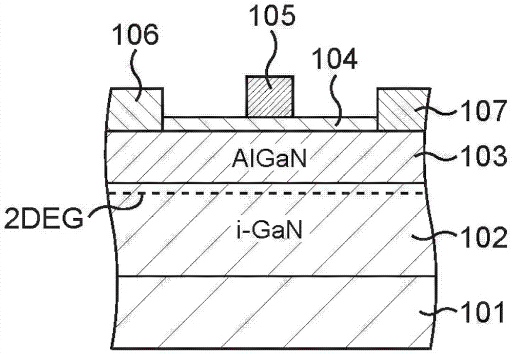
[0029] In the present embodiment, an AlGaN / GaN·HEMT of a nitride semiconductor is disclosed as a compound semiconductor device. Here, as an example, a so-called MIS-type AlGaN / GaN·HEMT in which a gate electrode is provided on a semiconductor through a gate insulating film is shown.
[0030] Figure 2A to Figure 2C with Figure 3A to Figure 3C is a schematic cross-sectional view showing a method of manufacturing the AlGaN / GaN·HEMT according to the first embodiment in process order.
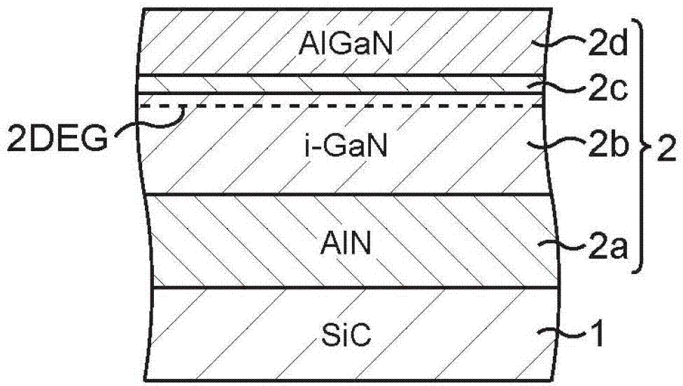
[0031] First, if Figure 2A As shown, a compound semiconductor stack structure 2 is formed on a semi-insulating SiC substrate 1 as a growth substrate, for example. As the growth substrate, a Si substrate, a sapphire substrate, a GaAs substrate, a GaN substrate, or the like may be used instead of the SiC substrate. Furthermore, the conductivity of the substrate can be semi-insulating or conductive.
[0032] The compound semiconductor stack structure 2 includes: a buffer layer 2a, an electron tr...
Embodiment )
[0062] Hereinafter, modified examples of the first embodiment will be explained. In this example, as in the first embodiment, the structure of the AlGaN / GaN·HEMT and its manufacturing method are disclosed, however, a so-called Schottky contact in which the gate electrode makes Schottky contact with the semiconductor is shown. type AlGaN / GaN·HEMT as an example. Note that the same constituent members and the like as those of the first embodiment will be denoted by the same reference numerals, and thus detailed description thereof will be omitted.
[0063] Figure 5A to Figure 5C as well as Figure 6A with Figure 6B is a schematic cross-sectional view showing the main process of the method of manufacturing the AlGaN / GaN·HEMT according to the modified example of the first embodiment.
[0064] First, similar to the first embodiment's Figure 2A with Figure 2B , forming a compound semiconductor stack structure 2 on the SiC substrate 1 . The compound semiconductor stack stru...
no. 2 approach )
[0085] The embodiment discloses the MIS-type AlGaN / GaN·HEMT and its manufacturing method as in the first embodiment, but the embodiment differs from the first embodiment in that the formation state of the passivation film is slightly different. Note that the same constituent members and the like as those of the first embodiment will be denoted by the same reference numerals, and thus detailed description thereof will be omitted.
[0086] Figure 7A to Figure 7C to Figure 9A with Figure 9B is a schematic cross-sectional view showing a method of manufacturing the AlGaN / GaN HEMT according to the second embodiment in process order.
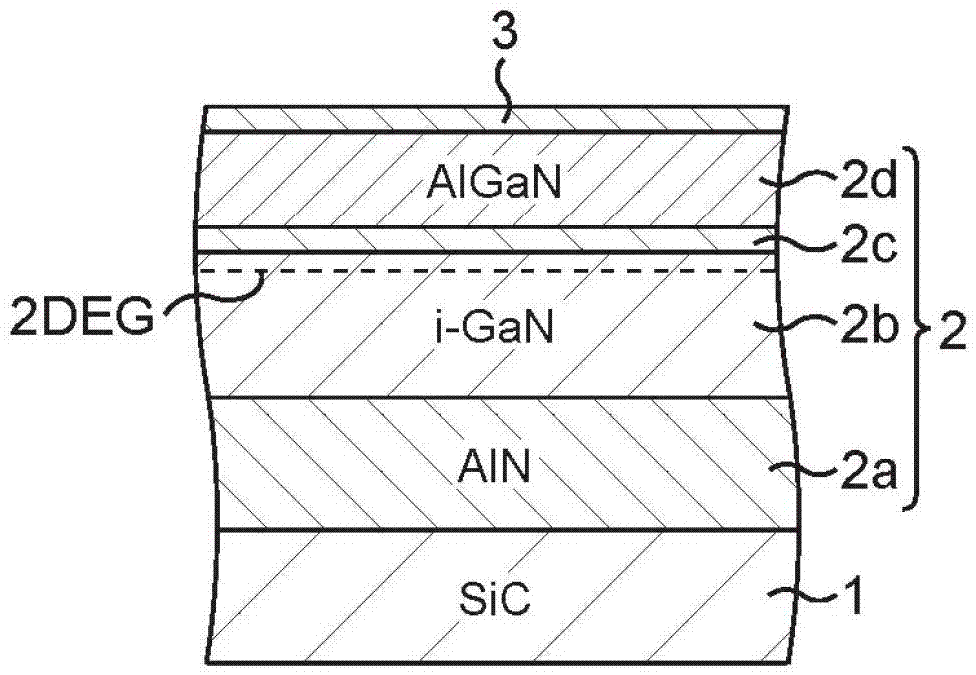
[0087] First, if Figure 7A As shown, a compound semiconductor stack structure 2 is formed on a semi-insulating SiC substrate 1 as a growth substrate, for example. The compound semiconductor stack structure 2 includes a buffer layer 2a, an electron transit layer 2b, an intermediate layer 2c, and an electron supply layer 2d. The method of growin...
PUM
 Abstract
Description
Claims
Application Information
 - R&D
- Intellectual Property
- Life Sciences
- Materials
- Tech Scout
- Unparalleled Data Quality
- Higher Quality Content
- 60% Fewer Hallucinations
Browse by: Latest US Patents, China's latest patents, Technical Efficacy Thesaurus, Application Domain, Technology Topic, Popular Technical Reports.
© 2025 PatSnap. All rights reserved.Legal|Privacy policy|Modern Slavery Act Transparency Statement|Sitemap|About US| Contact US: help@patsnap.com