Semiconductor device where logic region and DRAM are formed on same substrate

a logic region and semiconductor technology, applied in semiconductor devices, electrical devices, transistors, etc., can solve the problems of reducing the breakdown voltage, increasing the isub>off/sub>(degradation of retention characteristics) and the breakdown voltage, so as to reduce the word-line voltage in the peripheral circuit in the dram region, the breakdown voltage is sufficient, and the voltage applied to the first gate insulating film may be reduced.

Active Publication Date: 2013-11-05
RENESAS ELECTRONICS CORP
View PDF4 Cites 0 Cited by
  • Summary
  • Abstract
  • Description
  • Claims
  • Application Information

AI Technical Summary

Benefits of technology

[0036]The present inventors found out that, by configuring the first transistor to be applied with a negative bias voltage in the standby period, the word-line voltage may be reduced, and thereby also the voltage applied to the first gate insulating film may be reduced. Accordingly, a sufficient level of breakdown voltage may be ensured even if the equivalent oxide thickness T1 of the first gate insulating film of the first transistor in the DRAM region is thinned to fall in the above-described range. By virtue of this configuration, also the word-line voltage in the peripheral circuit in the DRAM region may be reduced.

Problems solved by technology

However, shrinkage in the gate size of the cell transistors in the DRAM region, and consequent adjustment of the thickness of the gate insulating film nearly equal to the thickness of the gate insulating film of the logic transistors, have raised problems of increase in Ioff (degradation in retention characteristics) and lowering in the breakdown voltage.

Method used


Image

  • Semiconductor device where logic region and DRAM are formed on same substrate
  • Semiconductor device where logic region and DRAM are formed on same substrate
  • Semiconductor device where logic region and DRAM are formed on same substrate

Examples


Embodiment Construction

[0041]The invention will be now described herein with reference to illustrative embodiments. Those skilled in the art will recognize that many alternative embodiments can be accomplished using the teachings of the present invention and that the invention is not limited to the embodiments illustrated for explanatory purposed.

[0042]Embodiments of the present invention will be described below referring to the attached drawings. Note that any similar constituents will be given with similar reference numerals or symbols in all drawings, and explanations therefor will not be repeated.

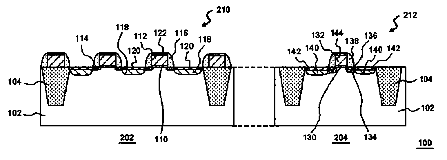
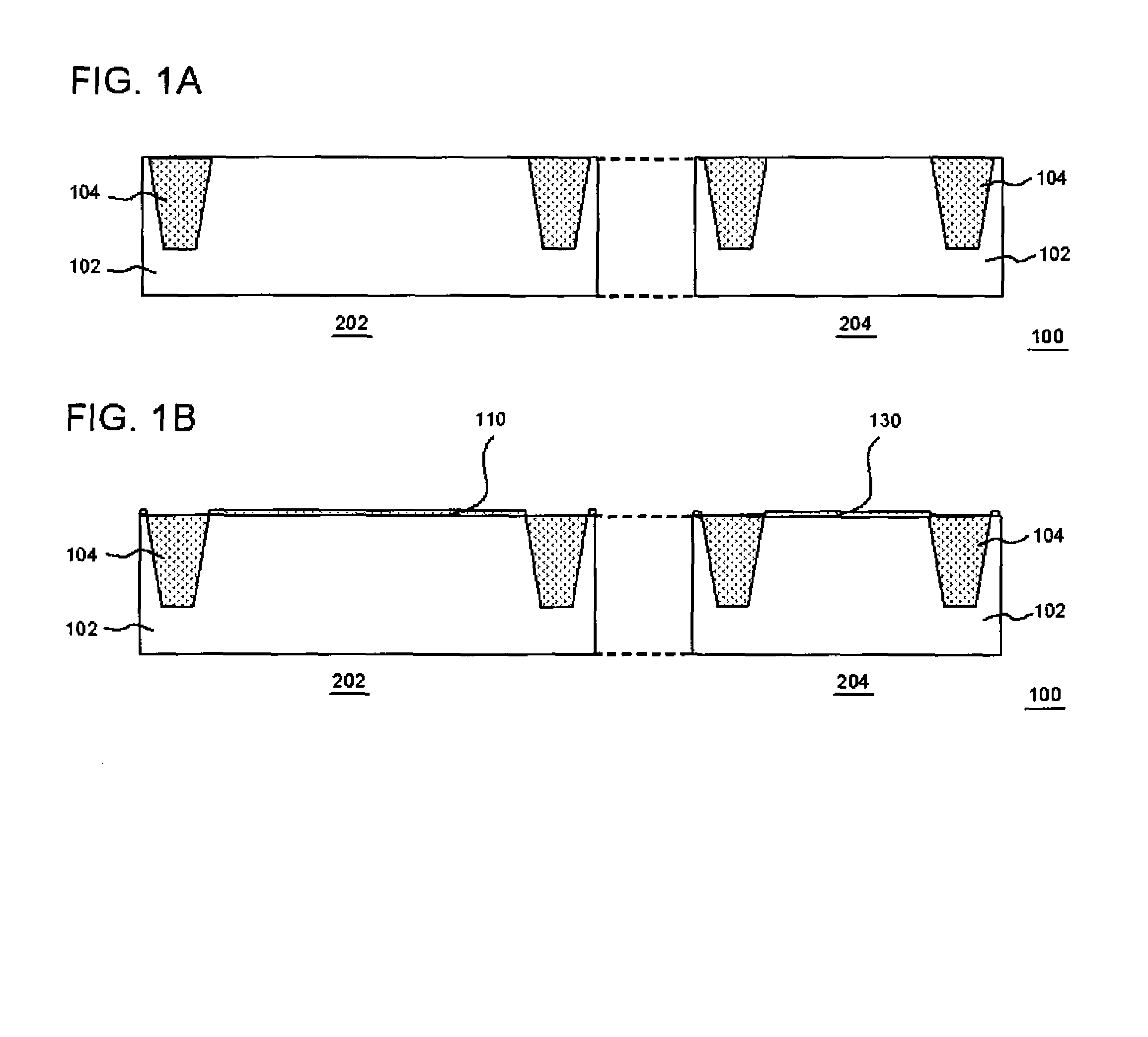
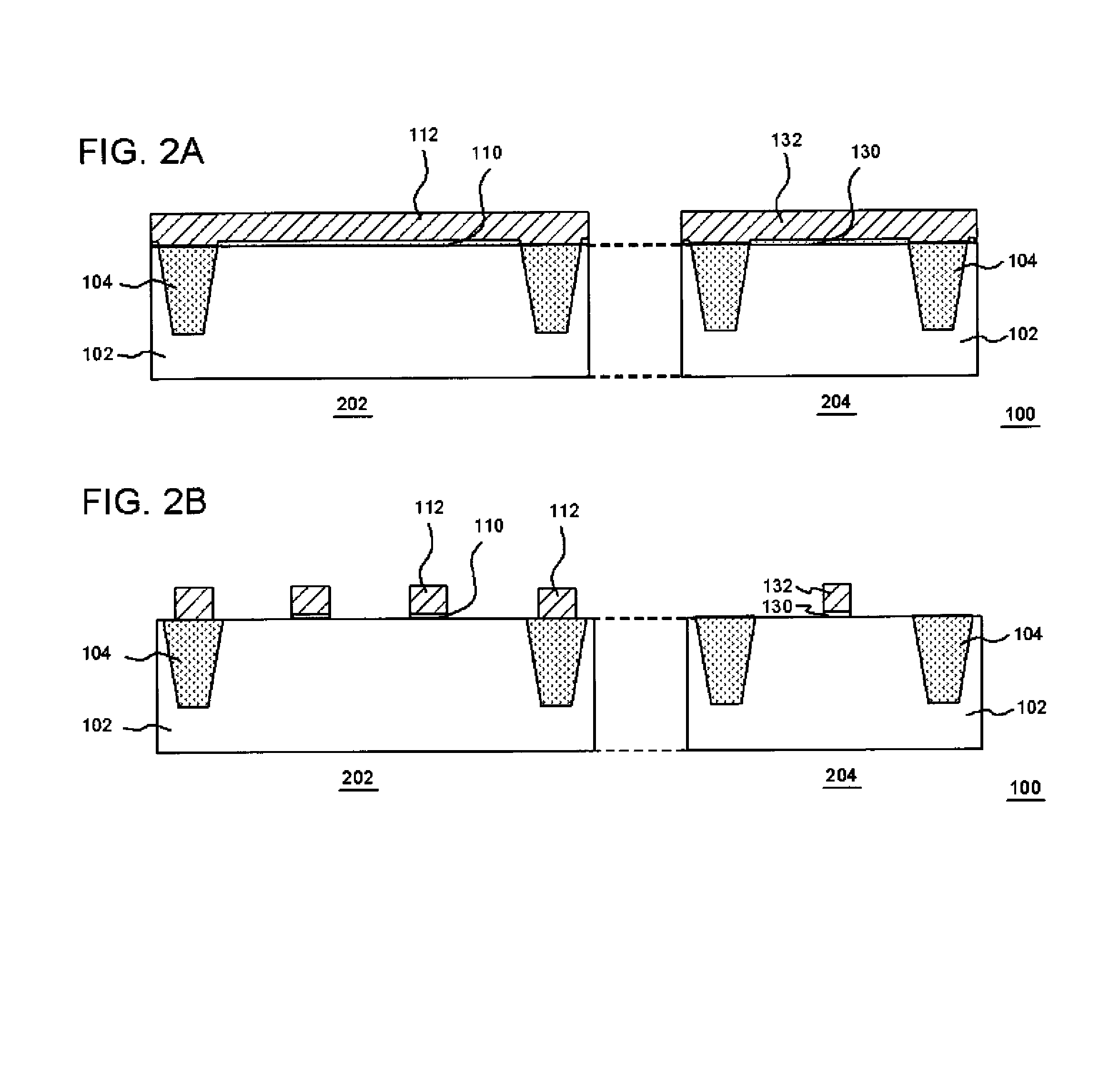
[0043]FIG. 1A to FIG. 4B are sectional views illustrating procedures of manufacturing a semiconductor device 100 of this embodiment. FIG. 5 is a plan view illustrating a configuration of the semiconductor device 100 of this embodiment.

[0044]In this embodiment, the semiconductor device 100 is a semiconductor device having a DRAM region 202 which contains DRAM cells, and a logic region 204.

[0045]As illustrated ...


PUM


Abstract

A semiconductor device having a DRAM region and a logic region embedded therein, includes: a substrate having the DRAM region and the logic region respectively formed thereon; a first transistor formed in the DRAM region, and having a first gate insulating film, and a second transistor formed in the logic region, and having a second gate insulating film, wherein equivalent oxide thickness T1 of the first gate insulating film of the first transistor is not larger than equivalent oxide thickness T2 of the second gate insulating film of the second transistor, the second transistor formed in the logic region has a pocket region which contains an impurity ion having a conductivity type different from that of an impurity ion composing the source/drain regions, while the first transistor formed in the DRAM region has no pocket region.

Description

BACKGROUND[0001]1. Technical Field[0002]The present invention relates to a semiconductor device (embedded DRAM) having a DRAM region and a logic region embedded therein.[0003]2. Related Art[0004]In a semiconductor device (embedded DRAM) having a DRAM region and a logic region embedded therein, transistors are formed in each of the DRAM region and the logic region so as to be adapted to the individual characteristics. In the conventional DRAM region, it has been necessary to make the gate insulating film thicker, in order to achieve a high breakdown voltage.[0005]The cells are, however, desired to be shrunk, for the purpose of increasing the memory capacity and reducing the cost. For this purpose, the gate length L and the gate width W of the cell transistors in the DRAM region are desired to be shrunk. On the other hand, it may be necessary to thin the gate insulating film (reduction in the equivalent oxide thickness (EOT)) in order to downsize the gates of the cell transistors in t...

Claims


Application Information

Patent Timeline
Patent Type & Authority Patents(United States)
IPC IPC(8): H01L29/78
CPCH01L27/10894H10B12/09
Inventor INOUE, KEN
Owner RENESAS ELECTRONICS CORP
Why Eureka
Try Eureka