Process for producing receiver substrate for semiconductor-on-insulator structure for radiofrequency applications and process for producing such structure

A technology of semiconductors and insulators, used in semiconductor/solid-state device manufacturing, electrical components, circuits, etc., and can solve problems such as breakdown voltage drop

Pending Publication Date: 2021-06-18
SOITEC SA
View PDF0 Cites 0 Cited by
  • Summary
  • Abstract
  • Description
  • Claims
  • Application Information

AI Technical Summary

Problems solved by technology

[0023] Therefore, fabricating substrates by reverse bonding results in a drop in the maximum electric field, which leads to a corresponding drop in the breakdown voltage

Method used


Image

  • Process for producing receiver substrate for semiconductor-on-insulator structure for radiofrequency applications and process for producing such structure
  • Process for producing receiver substrate for semiconductor-on-insulator structure for radiofrequency applications and process for producing such structure
  • Process for producing receiver substrate for semiconductor-on-insulator structure for radiofrequency applications and process for producing such structure

Examples


Embodiment Construction

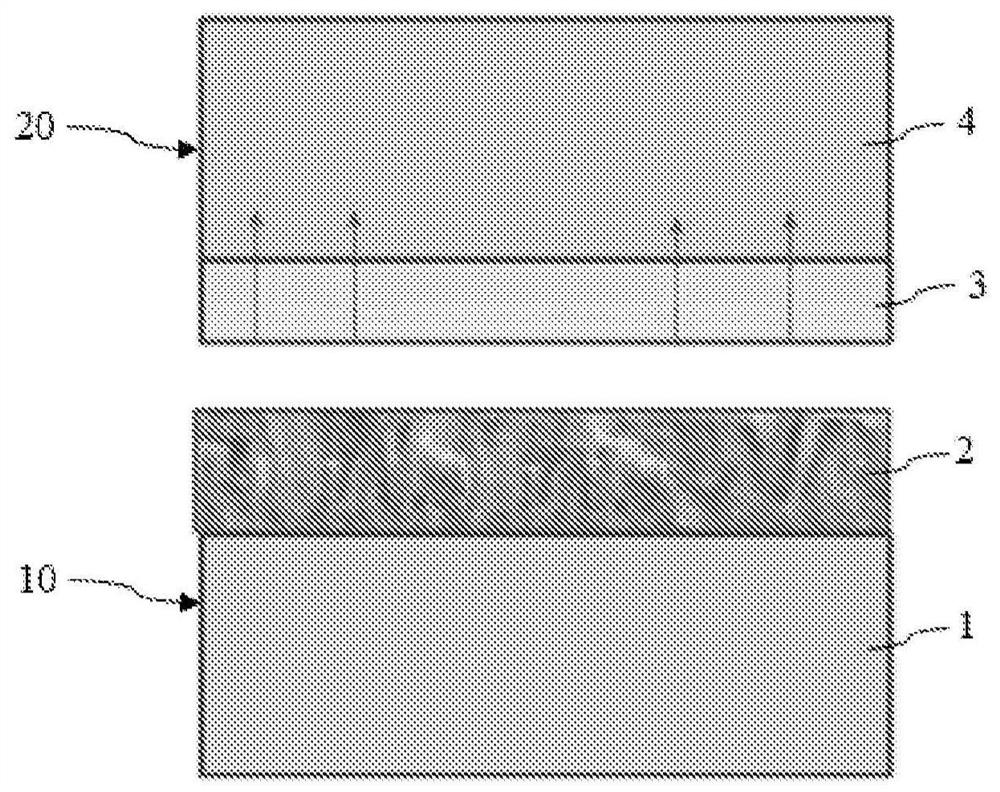
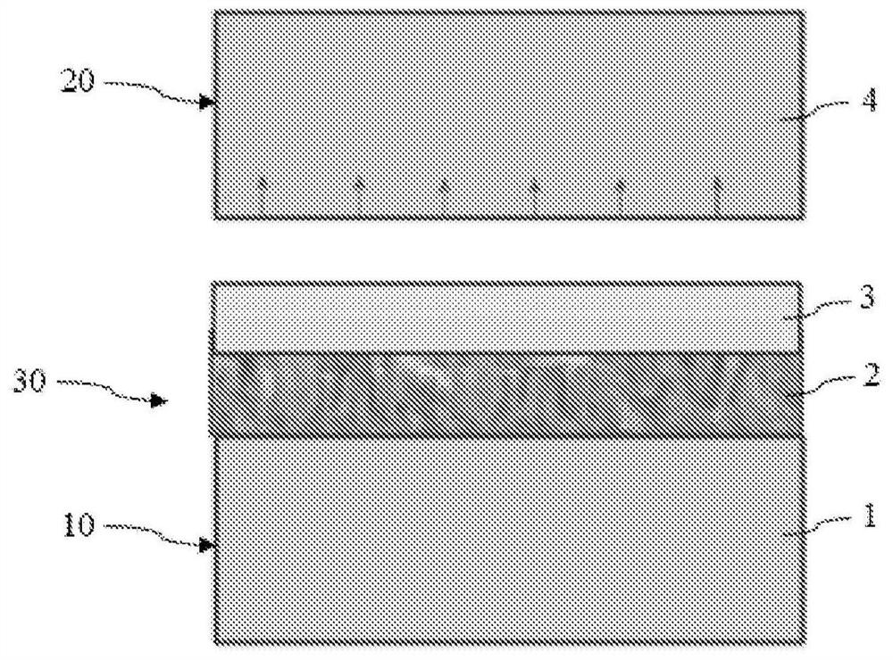
[0066] The invention relates to a method of manufacturing a receiver substrate (30) of a semiconductor-on-insulator structure for radio frequency applications, comprising the steps of:

[0067] The method of the present invention is a reverse splicing method. refer to figure 2 , the method includes the step of providing a semiconductor substrate 10 comprising a base substrate 1 made of a single crystal material and a charge-trapping layer 2 made of polysilicon disposed on the base substrate, followed by a pair of charges The trapping layer 2 is oxidized to form an oxide layer 3 disposed on said charge trapping layer.

[0068] The charge-trapping layer 2 may be formed by epitaxy on the base substrate 1, or alternatively deposited thereon by chemical vapor deposition (CVD).

[0069] The charge-trapping layer 2 is at least partially oxidized at a temperature comprised between 750°C and 875°C.

[0070] Such a method makes it possible to form, by reverse bonding, a receiver sub...


PUM

PropertyMeasurementUnit
thicknessaaaaaaaaaa
thicknessaaaaaaaaaa
thicknessaaaaaaaaaa

Abstract

The present invention relates to a process for producing a receiver substrate (30) for a semiconductor-on-insulator structure for radiofrequency applications. The method comprises the following steps of providing a semiconductor substrate comprising a base substrate (1) made of monocrystalline material and a charge-trapping layer (2) made of polycrystalline silicon arranged on the base substrate (1); oxidizing the charge-trapping layer (2) to form an oxide layer (3) arranged on the charge-trapping layer. The method is primarily characterized in that the oxidization of the charge-trapping layer (2) is performed at least partly at a temperature lower than or equal to 875 DEG C, in the following manner of starting the oxidization at a first temperature (T 1) between 750 DEG C and 1000 DEG C; decreasing the temperature down to a second temperature (T 2), lower than the first temperature (T 1), between 750 DEG C and 875 DEG C; continuing the oxidization at the second temperature (T 2).

Description

technical field [0001] The present invention relates to the fabrication of substrates known as "receiver substrates" for fabricating semiconductor-on-insulator structures for radio frequency applications. The invention also relates to a method of manufacturing such a structure by transferring a layer of a second substrate, called a "donor substrate", to a receiver substrate. Background technique [0002] In the context of fabricating a semiconductor-on-insulator structure (abbreviated SeOI), a donor substrate is bonded to a receiver substrate, a specific example of a semiconductor-on-insulator structure being a silicon-on-insulator (SOI) structure when the semiconductor is silicon. [0003] Typically, the provider substrate comprises a monocrystalline semiconductor substrate, such as a monocrystalline silicon substrate, while the recipient substrate comprises a substrate specifically intended to serve as a carrier for thin semiconductor layers that must be transferred from t...

Claims


Application Information

Patent Timeline
Patent Type & Authority Applications(China)
IPC IPC(8): H01L21/762H01L21/02H01L21/321
CPCH01L21/32105H01L21/76254H01L21/02002H01L21/02236
Inventor M·波卡特D·帕里西
Owner SOITEC SA
Why Eureka
Try Eureka