Pressure contact type semiconductor device having dummy segment
a semiconductor device and dummy segment technology, applied in semiconductor devices, semiconductor/solid-state device details, electrical devices, etc., can solve the problems of reducing the operational performance of gto thyristor, inability to achieve uniform step height, etc., to achieve stable operation performance and reduce yield
- Summary
- Abstract
- Description
- Claims
- Application Information
AI Technical Summary
Benefits of technology
Problems solved by technology
Method used
Image

Examples
first preferred embodiment
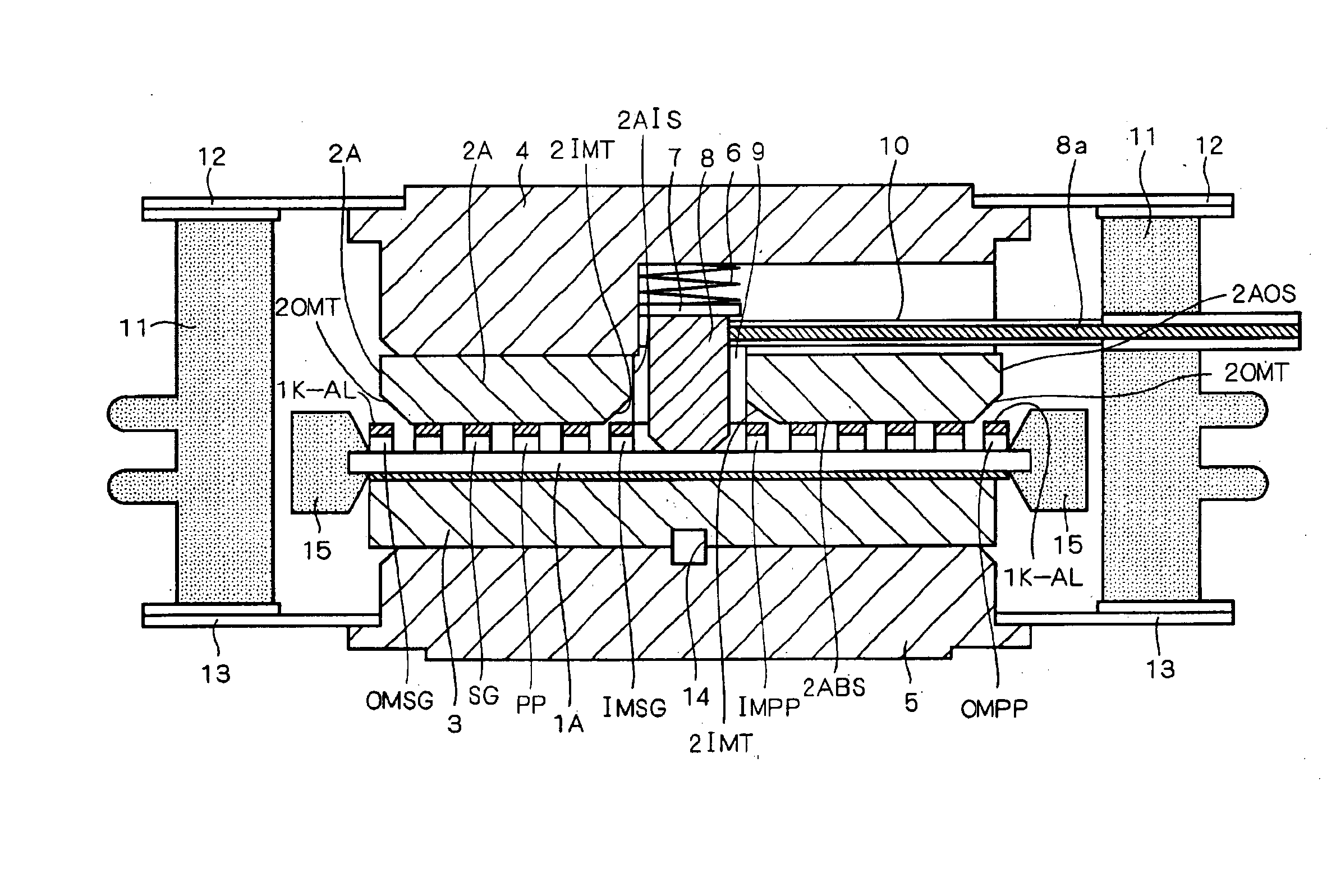
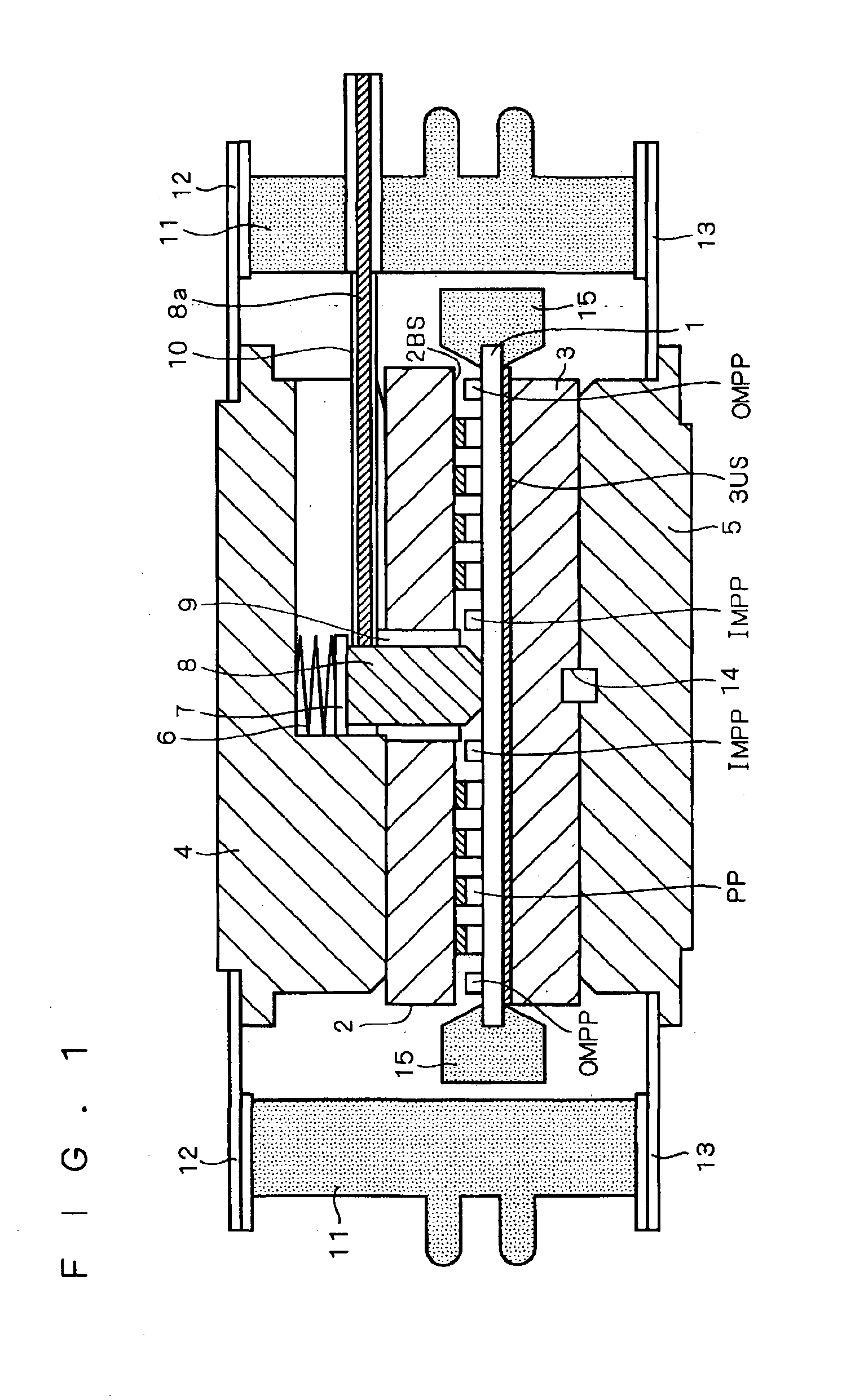
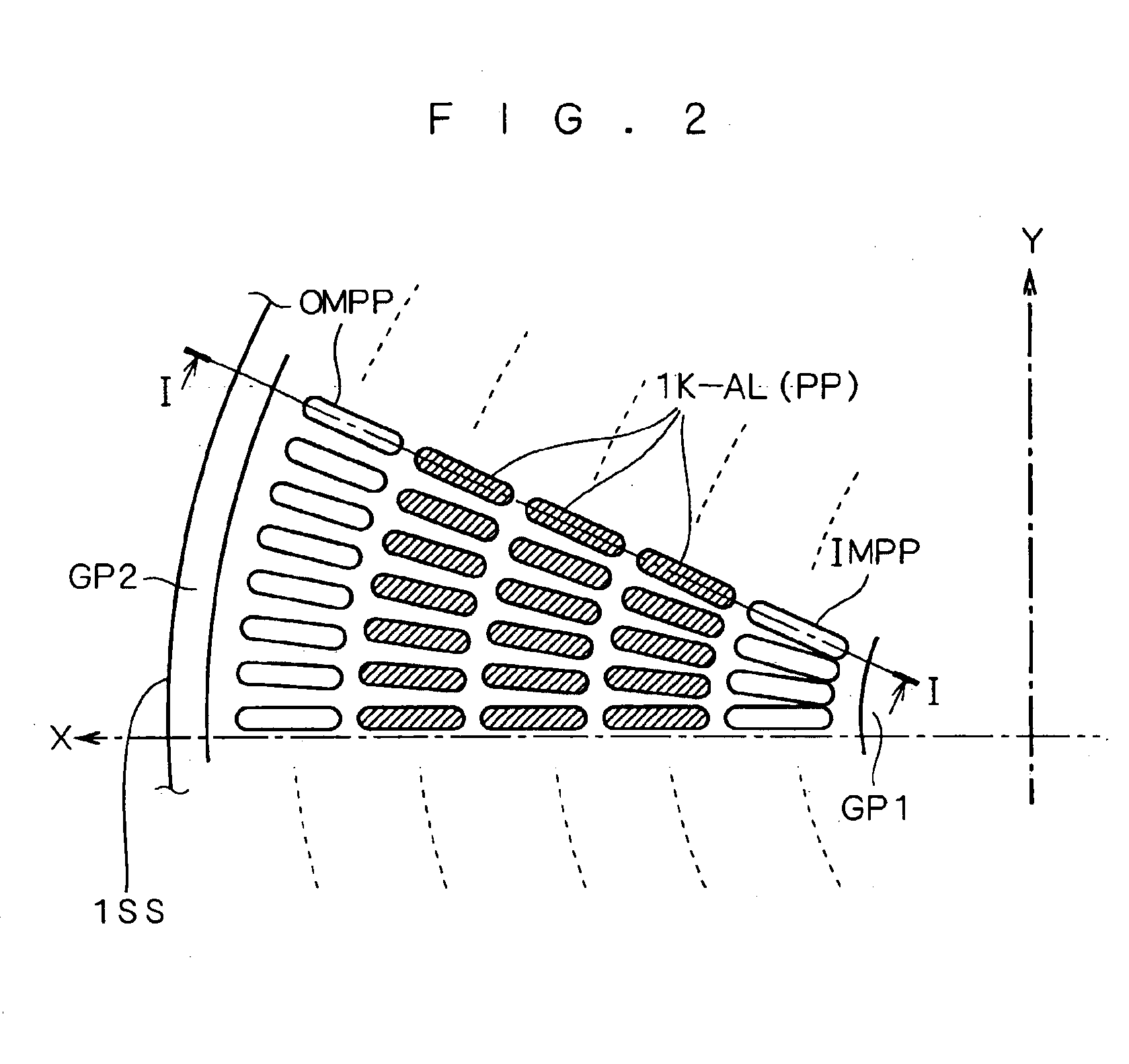
FIG. 1 is a longitudinal sectional view of a structure of a pressure contact type semiconductor device according to the first preferred embodiment. In FIG. 1, a GTO thyristor of a center gate type is shown as a non-limiting example of the pressure contact type semiconductor device according to the first preferred embodiment. FIG. 2 is a plan view of a first main surface of a cylindrical semiconductor substrate 1 illustrated in FIG. 1. In FIG. 2, illustration of a gate electrode 1G-AL is omitted. It is noted that the first main surface is a top surface of the semiconductor substrate 1, which includes exposed regions of a third top surface of a third semiconductor layer (P-type base layer) PB and exposed surfaces of fourth semiconductor layers (N-type emitter layer) NE. The whole of a fourth bottom surface of each of the fourth semiconductor layers NE is contributed to formation of a PN junction between the third semiconductor layer PB and each of the fourth semiconductor layers NE as...
first modification
Referring to an arrangement pattern of the cathode electrodes as illustrated in FIG. 4, an area of each of the outermost and innermost protruding portions OMPP and IMPP in the dummy segments is determined to be smaller than an area of each of the other protruding portions PP.
This makes it possible to increase an area of each of the other operational segments (non-dummy segments or active segments). Accordingly, a contact area between each of the cathode electrodes 1K-AL and the bottom surface 2BS of the cathode strain relief plate 2 can be maximized.
Alternatively, an area of only each outermost protruding portion OMPP or only each innermost protruding portion IMPP may be made smaller than an area of each of the other protruding portions PP.
second modification
Referring to an arrangement pattern of the cathode electrodes as illustrated in FIG. 5, respective shapes of the outermost protruding portions OMPP in the dummy segments are determined to be continuous with one another so as to form a single ring, and respective shapes of the innermost protruding portions IMPP in the dummy segments are determined to be continuous with one another so as to form another single ring.
By employing a single ring-shaped protruding portion formed of protruding portions which are arranged continuously with one another along an entire circumference of a semiconductor substrate, it is possible to suppress photographic defects possibly caused during photolithography (pin holes or variation in thickness of resist). Also, each of a single ring-shaped protruding portion formed of the outermost protruding portions OMPP and a single ring-shaped protruding portion formed of the innermost protruding portions IMPP can function as a barrier wall for preventing a foreign...
PUM
 Abstract
Description
Claims
Application Information
 - R&D
- Intellectual Property
- Life Sciences
- Materials
- Tech Scout
- Unparalleled Data Quality
- Higher Quality Content
- 60% Fewer Hallucinations
Browse by: Latest US Patents, China's latest patents, Technical Efficacy Thesaurus, Application Domain, Technology Topic, Popular Technical Reports.
© 2025 PatSnap. All rights reserved.Legal|Privacy policy|Modern Slavery Act Transparency Statement|Sitemap|About US| Contact US: help@patsnap.com