Method and apparatus for fabrication of large area 3D photonic crystals with embedded waveguides

a technology of waveguides and photonic crystals, applied in the field of photonic crystals, can solve the problems of z-) pitches, reducing the available range of (x-, y-) pitches, and reducing the cost of manufacturing

Active Publication Date: 2015-10-06
STC UNM
View PDF5 Cites 12 Cited by
  • Summary
  • Abstract
  • Description
  • Claims
  • Application Information

AI Technical Summary

Benefits of technology

[0031]In some aspects of the present disclosure, a method of fabricating a three-dimensional (3D) photonic crystal comprising using a multiple-exposure, two-beam interferometric lithography (IL) arrangement is disclosed. The multiple-exposure method can comprise tilting, with the centerline between the two beams tilted relative to the surface no...

Problems solved by technology

The ion-milling and woodpile approaches are process intensive and have alignment or inter-level registration issues.
An issue in conventional multi-beam (typically 4 or 5 beams) approaches to 3D IL is that the z-pitch is constrained by the physics of the optical configuration and is typically much larger than the (x-, y-) pitches, for cases where the exposure wavelength is much short...

Method used


Image

  • Method and apparatus for fabrication of large area 3D photonic crystals with embedded waveguides
  • Method and apparatus for fabrication of large area 3D photonic crystals with embedded waveguides
  • Method and apparatus for fabrication of large area 3D photonic crystals with embedded waveguides

Examples


Embodiment Construction

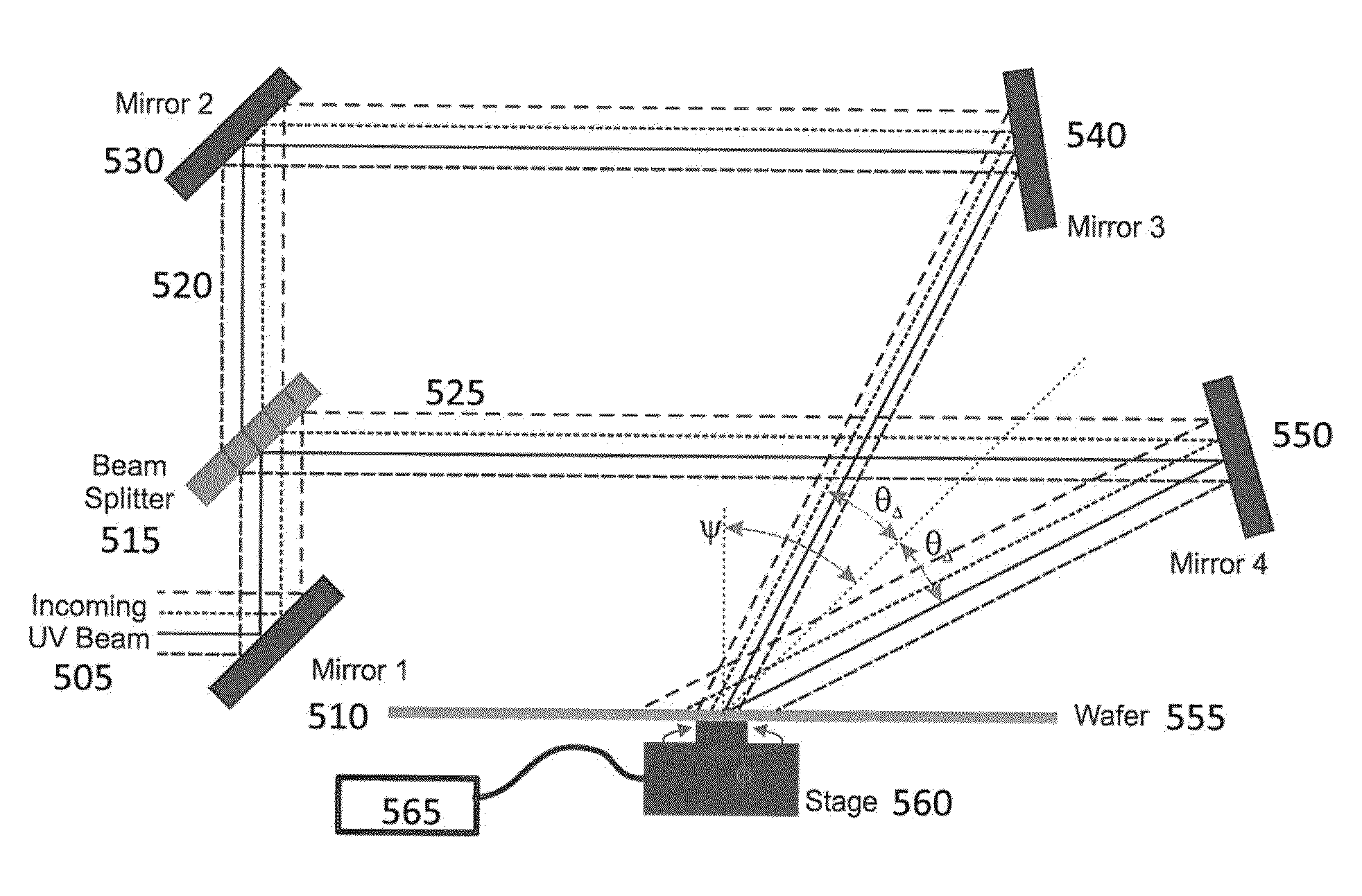
[0061]Reference will now be made in detail to the exemplary embodiments of the invention, examples of which are illustrated in the accompanying drawings. Wherever possible, the same reference numbers will be used throughout the drawings to refer to the same or like parts. In the following description, reference is made to the accompanying drawings that form a part thereof, and in which is shown by way of illustration specific exemplary embodiments in which the invention may be practiced. These embodiments are described in sufficient detail to enable those skilled in the art to practice the invention and it is to be understood that other embodiments may be utilized and that changes may be made without departing from the scope of the invention. The following description is, therefore, merely exemplary.

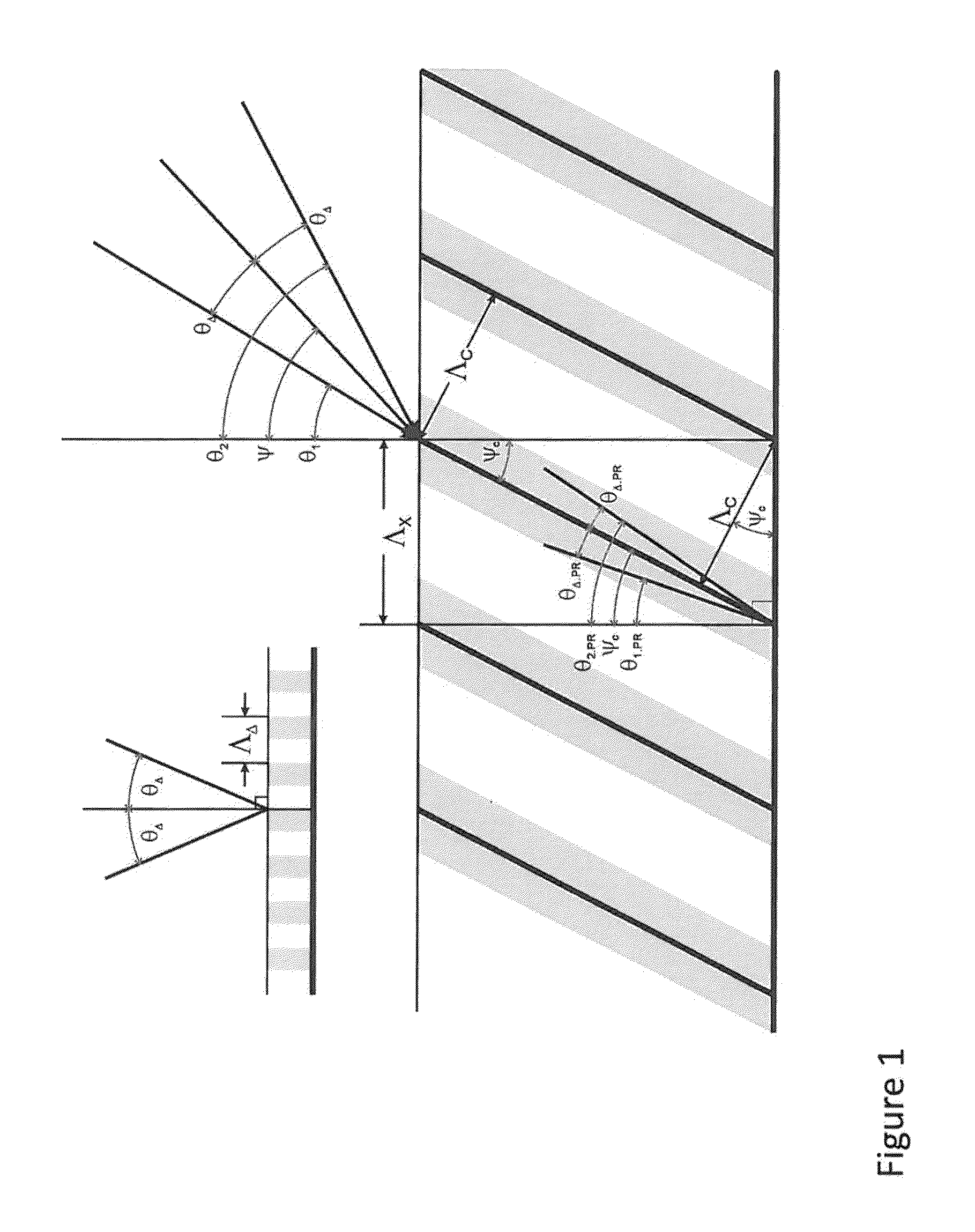
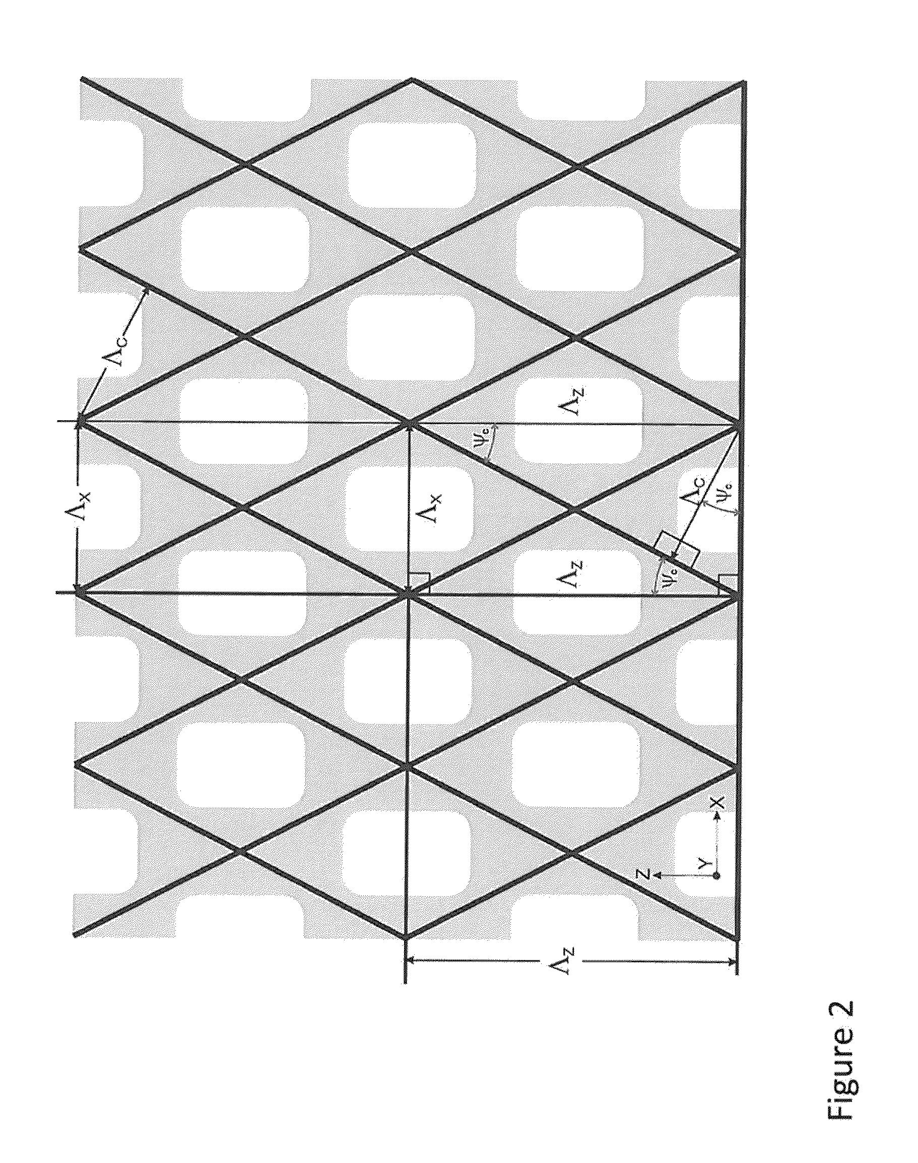
[0062]The 3D photonic crystals can be formed by a multiple exposure two-beam interferometric lithography technique, which allows for independent dimensional control of the period along e...


PUM

PropertyMeasurementUnit
Angleaaaaaaaaaa
Angleaaaaaaaaaa
Angleaaaaaaaaaa

Abstract

In accordance with some aspects of the present disclosure, a maskless interferomeric lithography system for fabricating a three-dimensional (3D) photonic crystal using a multiple two-beam-exposures is disclosed. The system can comprise an illumination system comprising an optical arrangement operable to receive radiation from a radiation source and provide three or more tilted two-beam interference pattern exposures to be combined into a three-dimensional pattern; and a substrate operable to be supported by a substrate table, wherein the substrate comprises a photoresist formed on a top surface of the substrate and operable to receive the three-dimensional pattern and wherein means are provided to adjust the position of the substrate in all six mechanical degrees of freedom.

Description

CROSS REFERENCE TO RELATED APPLICATIONS[0001]This application claims priority to U.S. Provisional Patent Application No. 61 / 439,722 filed on Feb. 4, 2011, which is hereby incorporated in its entirety by reference.GOVERNMENT INTEREST[0002]This invention was made with U.S. Government support under Contract No. FA9550-09-100202 awarded by the Air Force Office of Scientific Research. As a result the U.S. Government has certain rights in this invention.FIELD OF THE INVENTION[0003]This invention relates generally to photonic crystals and, more particularly, to materials and methods of large area three-dimensional (3D) photonic crystals and to waveguides embedded within the 3D photonic crystals.BACKGROUND OF THE INVENTION[0004]A three-dimensional (3D) crystal has a periodic dielectric function in all three orthogonal Cartesian directions (x, y, z-axes). 3D photonic crystals are attractive for very compact waveguide devices. There are numerous ways to fabricate 3D photonic crystals (PhCs) i...

Claims


Application Information

Patent Timeline
IPC IPC(8): G03F7/20G03F7/00C03B37/01
CPCG03F7/0005C03B37/01G03F7/70408B82Y20/00G02F2202/32G03F7/2022G03F7/2041G03F7/32G03F7/40
Inventor BRUECK, STEVEN R. J.RAUB, ALEXANDER K.
Owner STC UNM
Why Eureka
Try Eureka