Voltage-controlled magnetic memory element with canted magnetization
a magnetic memory element and voltage control technology, applied in the field of magnetic tunnel junctions, can solve problems such as limiting the energy efficiency of spintronic memory and logic devices
- Summary
- Abstract
- Description
- Claims
- Application Information
AI Technical Summary
Benefits of technology
Problems solved by technology
Method used
Image
Examples
experiment # 1
[0056]Experiment #1
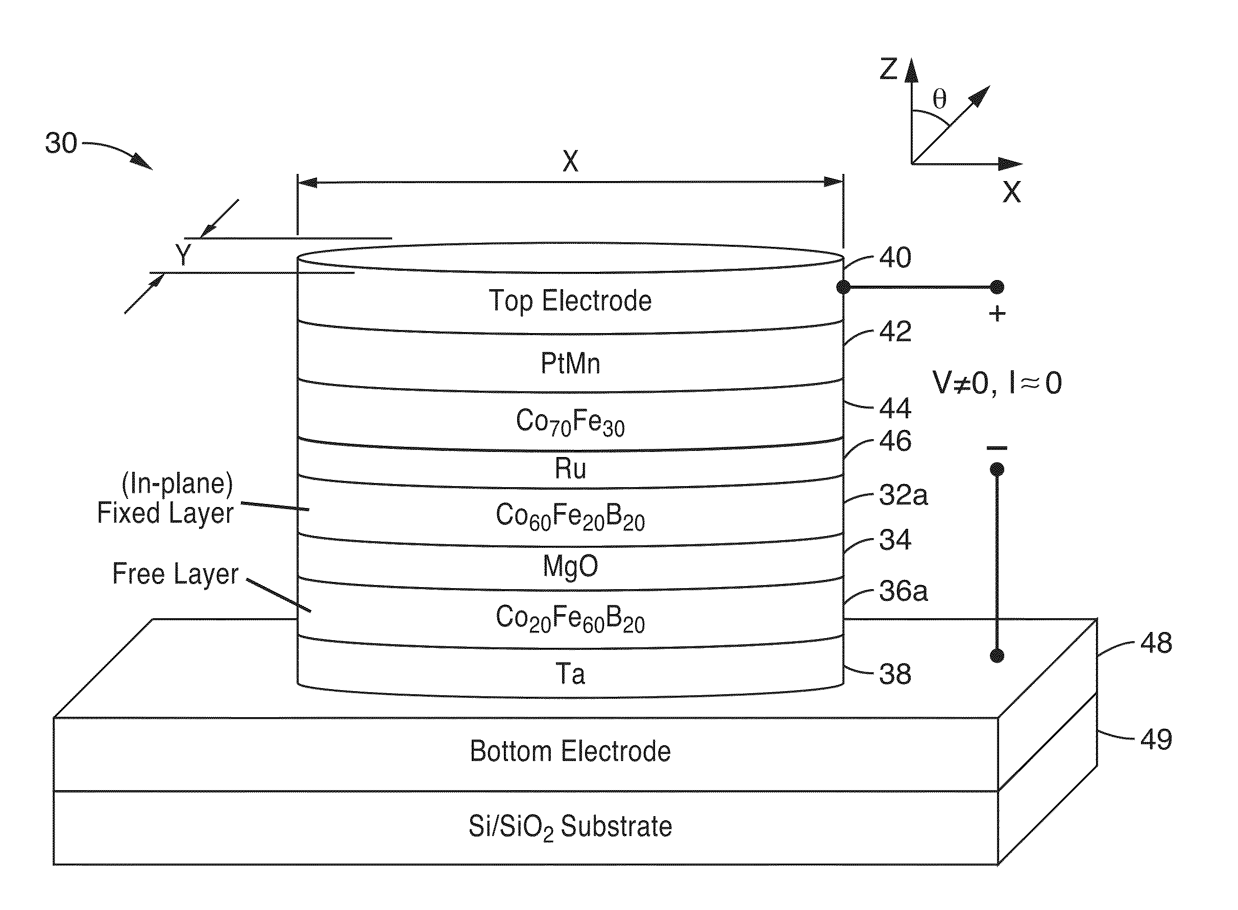
[0057]To test the devices of the present invention detailed above, continuous multilayer films with a composition similar to that shown in FIG. 3A (e.g. substrate 49 / bottom electrode 48 / Ta (5 nm thickness) / Co20Fe60B20 free layer 36a with thickness range(tCoFeB=1.0 nm-1.4 nm wedge) / MgO dielectric layer 34 with thickness range (tMgO=1.2 nm-1.4 nm wedge) / Co60Fe20B20 in-plane fixed layer 32a (2.7 nm thickness) / Ru layer 46 (0.85 nm thickness) / Co70Fe30 layer 44 (2.3 thickness) / PtMn layer 42 (20 nm thickness) / top electrode 40 were deposited in a Singulus TIMARIS physical vapor deposition (PVD) system, and subsequently annealed at 300° C. for 2.0 hours in an in-plane magnetic field of 1 T. The films were then patterned into 170 nm×60 nm elliptical nanopillars for electrical measurements using electron-beam lithography and ion milling techniques. The readout of the state of the free layer is performed via the TMR effect and all the measurements were performed at room tempe...
PUM
 Abstract
Description
Claims
Application Information
 - R&D
- Intellectual Property
- Life Sciences
- Materials
- Tech Scout
- Unparalleled Data Quality
- Higher Quality Content
- 60% Fewer Hallucinations
Browse by: Latest US Patents, China's latest patents, Technical Efficacy Thesaurus, Application Domain, Technology Topic, Popular Technical Reports.
© 2025 PatSnap. All rights reserved.Legal|Privacy policy|Modern Slavery Act Transparency Statement|Sitemap|About US| Contact US: help@patsnap.com


