Semiconductor circuit, method for driving the same, storage device, register circuit, display device, and electronic device
a technology of semiconductor circuits and circuits, applied in the direction of transistors, static indicating devices, instruments, etc., can solve the problems of difficult to control the threshold voltage of transistors properly, and the threshold voltage of transistors can be changed, so as to achieve low power consumption, and markedly reduced power consumption
- Summary
- Abstract
- Description
- Claims
- Application Information
AI Technical Summary
Benefits of technology
Problems solved by technology
Method used
Image
Examples
embodiment 1
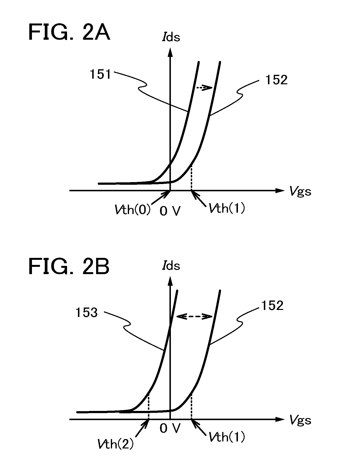
[0051]In this embodiment, examples of a semiconductor circuit capable of controlling the threshold voltage of a transistor in the present invention are described with reference to FIGS. 1A and 1B, FIGS. 2A and 2B, and FIGS. 3A and 3B.
Structure Example
[0052]FIG. 1A illustrates a control circuit 100 in this embodiment and a transistor 111 connected to the control circuit 100.
[0053]The transistor 111 includes a back gate (a second gate electrode), and output voltage from the control circuit 100 is input to the back gate. Although an n-channel transistor is used as the transistor 111 in this embodiment, a p-channel transistor can be used.
[0054]The control circuit 100 includes a diode 101, a capacitor 103, and a capacitor 105. An input terminal IN is connected to the control circuit 100. A second electrode of the diode 101 is connected to an input portion, and a first electrode of the diode 101 is connected to a first electrode of the capacitor 103. A second electrode of the capacitor 10...
modification example
[0069]Here, the diode 101 included in the control circuit 100 can be formed using a transistor. FIGS. 3A and 3B each illustrate an example in which a transistor is used as the diode included in the control circuit.
[0070]For example, in the control circuit 100 in FIG. 3A, a transistor 107 whose first electrode is connected to the input terminal IN and whose second electrode and gate electrode are connected to the node (A) can be used as a diode, as illustrated in FIG. 3A. Alternatively, as illustrated in FIG. 3B, a transistor 109 including a back gate may be used and two gate electrodes of the transistor 109 may be connected to the node (A). By connection of the back gate in addition to the gate electrode with the node (A), the current value at the time of application of forward bias can be increased, and the time for input of the first input signal can be shortened. Further, leakage current at the time of application of reverse bias can be suppressed, so that the hold time of the vo...
embodiment 2
[0077]In this embodiment, a structure example where the semiconductor circuit capable of controlling the threshold voltage of a transistor in Embodiment 1 is used as a register circuit that is one of storage devices is described with reference to FIGS. 4A and 4B.
Structure Example
[0078]FIG. 4A illustrates a structure example of a 1-bit register circuit to which the control circuit 100 in Embodiment 1 is connected. A register circuit 200 includes a transistor 201, a capacitor 203, and a flip-flop circuit 205. In this embodiment, an n-channel transistor is used as the transistor 201.
[0079]The transistor 201 includes a back gate (a second gate electrode) as in the transistor 111 in Embodiment 1, and output voltage from the control circuit 100 is input to the back gate. An input terminal Sig1 is connected to a first gate electrode of the transistor 201, an input terminal Sig2 is connected to a first electrode of the transistor 201, and the transistor 201 is controlled with input signals ...
PUM
 Abstract
Description
Claims
Application Information
 - R&D
- Intellectual Property
- Life Sciences
- Materials
- Tech Scout
- Unparalleled Data Quality
- Higher Quality Content
- 60% Fewer Hallucinations
Browse by: Latest US Patents, China's latest patents, Technical Efficacy Thesaurus, Application Domain, Technology Topic, Popular Technical Reports.
© 2025 PatSnap. All rights reserved.Legal|Privacy policy|Modern Slavery Act Transparency Statement|Sitemap|About US| Contact US: help@patsnap.com


