Laser processing method
a laser processing and laser technology, applied in the field of laser processing methods, can solve problems such as cutting error, and achieve the effect of reducing the number of manufacturing steps and high precision
- Summary
- Abstract
- Description
- Claims
- Application Information
AI Technical Summary
Benefits of technology
Problems solved by technology
Method used
Image
Examples
first example
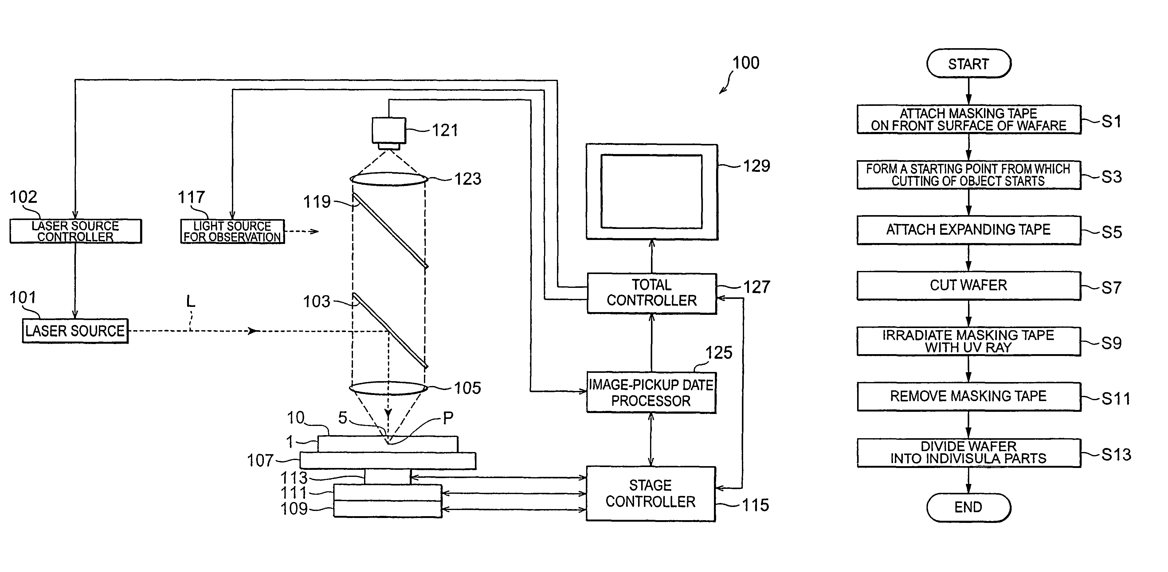
[0117]FIGS. 18 and 19 are flowcharts for explaining a first example of the laser processing method in accordance with the embodiment. FIGS. 20 to 22 are sectional views of the wafer 1a for explaining the laser processing method in accordance with this example.
[0118]Referring to FIG. 18, a protective tape 25 as a protective film for protecting a laminate 4 is initially attached to the front face 3 of the wafer 1a (S1, FIG. 20A). Various materials can be used as a material for the protective tape 25 as long as they have a cushioning effect for protecting the laminate part 4 and do not affect operating characteristics of the laminate part 4. Chosen as the material for the protective tape 25 in this embodiment is one which can absorb shocks while being removable when irradiated with UV rays.
[0119]Subsequently, a cutting start region 8 is formed within the substrate 15 of the wafer 1a along a line 5 along which the object is intended to be cut (S3, FIG. 20B). The wafer 1a shown in FIG. 2...
second example
[0140]FIG. 24 is a flowchart showing a second example of the laser processing method in accordance with this embodiment. FIGS. 25 to 27 are sectional views of the wafer 1a for explaining this example. This example differs from the above-mentioned first example in three points, i.e., (1) that the substrate is shaved so as to become thinner; (2) that no breaking with the knife edge 33 or the like is effected; and (3) that the protective tape 25 is peeled off after dividing the wafer 1a into a plurality of chip parts 24.
[0141]Referring to FIG. 24, the protective tape 25 is initially attached to the front face 3 of the wafer 1a (S21, FIG. 25A). This step is the same as the step S1 in the first example and thus will not be explained in detail.
[0142]Subsequently, the rear face 21 of the wafer 1a is shaved (S23, FIG. 25B). Here, the substrate 15 is shaved (ground) until it has a thickness of 30 μm to 50 μm, for example. In order for the laser light L to be favorably made incident on the re...
third example
[0151]FIG. 28 is a flowchart showing a third example of the laser processing method in accordance with this embodiment. This example differs from the above-mentioned first example in one point, i.e., (1) that the breaking with the knife edge 33 or the like is not effected. This modified example will be explained with reference to FIGS. 20 to 22 which are shown in the first example.
[0152]Referring to FIG. 28, the protective tape 25 is initially attached to the front face 3 of the wafer 1a (S41, FIG. 20A). Subsequently, the cutting start region 8 is formed within the substrate 15 of the wafer 1a along the line 5 along which the object is intended to be cut (S43, FIG. 20B). Then, the expandable tape 23 is attached to the rear face 21 of the wafer 1a (S45, FIG. 20C). These steps are the same as the steps S1 to S5 in the above-mentioned first example, respectively, and thus will not be explained in detail.
[0153]Next, the protective tape 25 is irradiated with UV rays (S47, FIG. 21B), and ...
PUM
| Property | Measurement | Unit |
|---|---|---|
| outer diameter | aaaaa | aaaaa |
| thickness | aaaaa | aaaaa |
| size | aaaaa | aaaaa |
Abstract
Description
Claims
Application Information
 - R&D
- Intellectual Property
- Life Sciences
- Materials
- Tech Scout
- Unparalleled Data Quality
- Higher Quality Content
- 60% Fewer Hallucinations
Browse by: Latest US Patents, China's latest patents, Technical Efficacy Thesaurus, Application Domain, Technology Topic, Popular Technical Reports.
© 2025 PatSnap. All rights reserved.Legal|Privacy policy|Modern Slavery Act Transparency Statement|Sitemap|About US| Contact US: help@patsnap.com


