
Methods for improving double patterning route efficiency

Inactive Publication Date: 2014-11-04
GLOBALFOUNDRIES INC
View PDF5 Cites 17 Cited by
  • Summary
  • Abstract
  • Description
  • Claims
  • Application Information

AI Technical Summary

Benefits of technology

The present invention provides a method for designing an integrated circuit by arranging a plurality of cells with metal lines and an intercell region between them, identifying metal layer lines that can have a jog applied to them, and applying the jog to the metal layer lines. This results in faster and more efficient design of integrated circuits, particularly with advanced technologies. An integrated circuit designed using this method can also have a metal layer line with a jog, which improves the performance of the circuit.

Problems solved by technology

However, the ability to project an accurate image of increasingly smaller features onto the wafer is limited by the wavelength of the light used and the ability of the lens system.
Unrestricted routing layout may result in “color conflicts” which violate DPT design rules.
Resolving these conflicts to render a pattern DPT compatible may be computationally intensive and may also require significant re-layout of the pattern, which can significantly increase cost.
As more complicated designs are developed to achieve higher performance and higher reliability in a smaller chip area, the demands placed on routing tools increase.

Method used


Image

  • Methods for improving double patterning route efficiency
  • Methods for improving double patterning route efficiency
  • Methods for improving double patterning route efficiency

Examples


Embodiment Construction

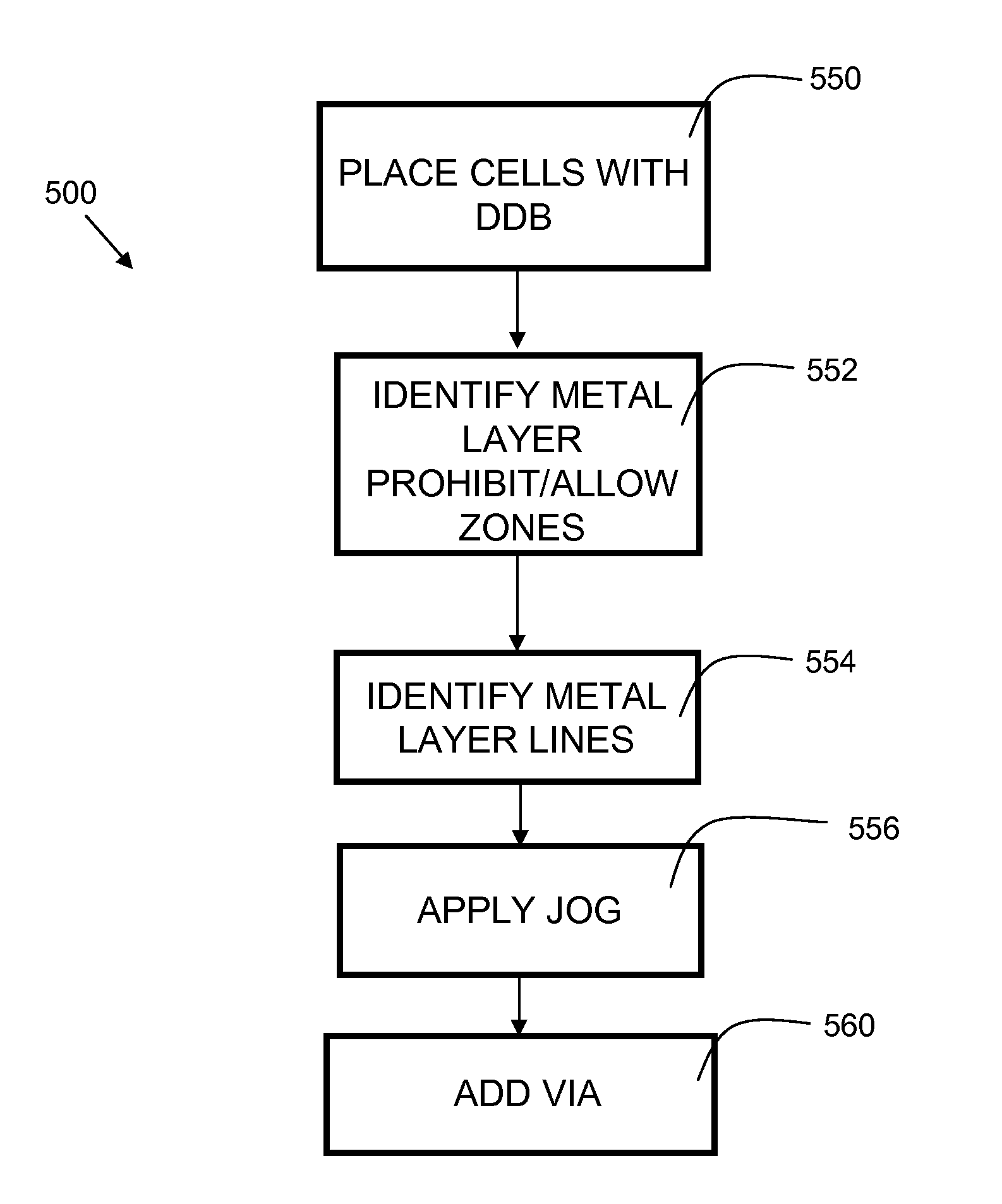
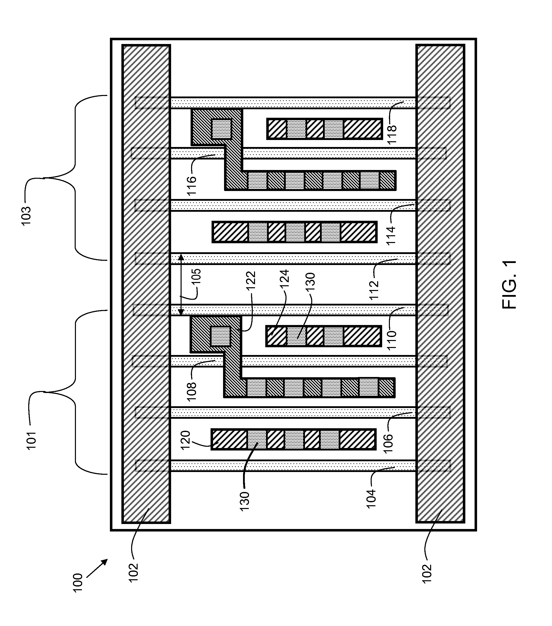
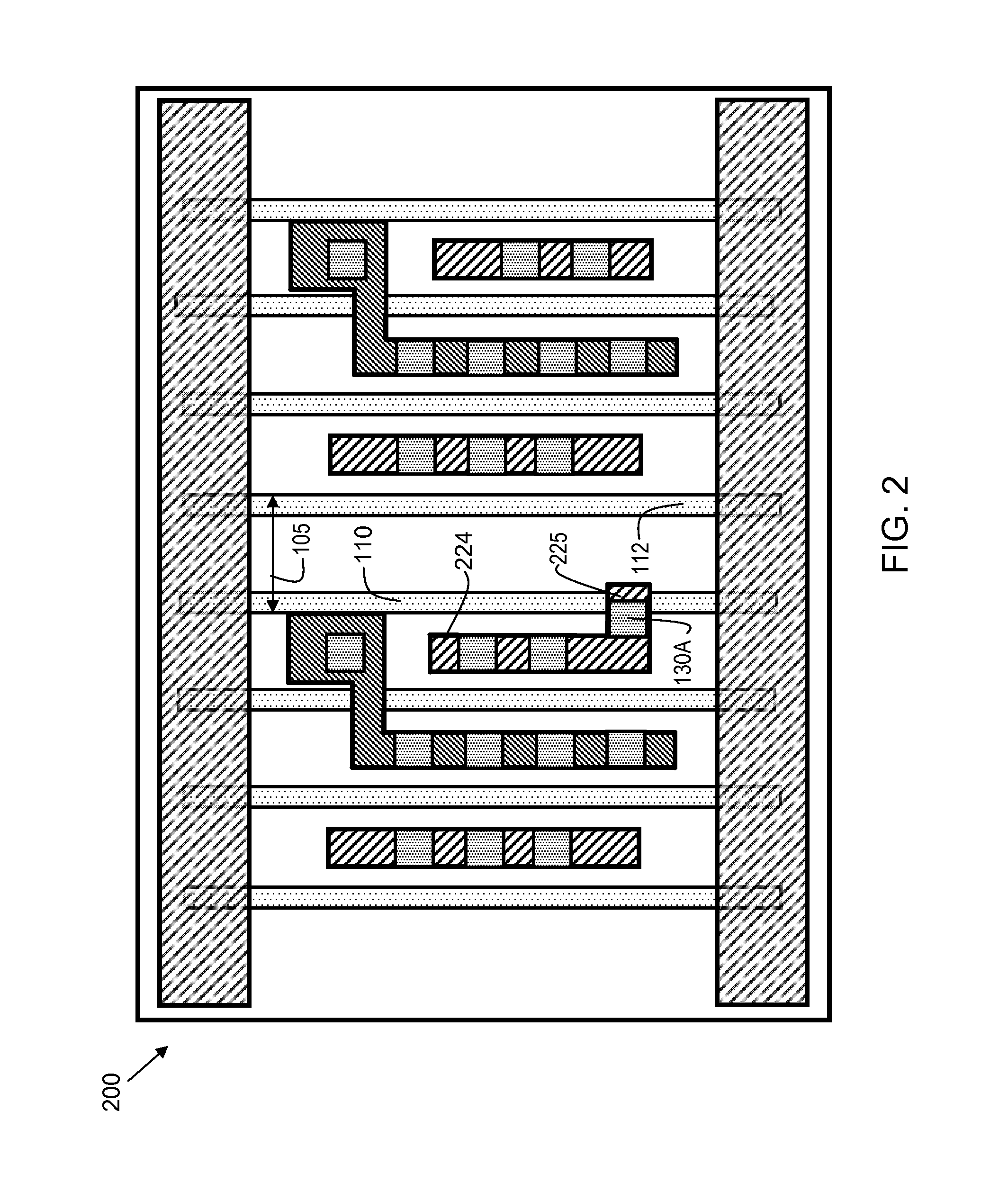
[0018]Exemplary embodiments will now be described more fully herein with reference to the accompanying drawings, in which exemplary embodiments are shown. Embodiments of the present invention provide a design methodology that improves routing for an integrated circuit. The placed cells include double diffusion breaks. A double diffusion break (DDB) refers to a standard cell architecture where the cell boundary is tucked under a dummy polysilicon gate line. Use of cells with a double diffusion break can provide more uniform transistor performance and better design performance. Metal layer 1 (M1) prohibit zones are defined to prohibit any M1 structures in the prohibit zones. This facilitates adding additional vias and / or viabars to improve circuit performance and product yield.

[0019]It will be appreciated that this disclosure may be embodied in many different forms and should not be construed as limited to the exemplary embodiments set forth herein. Rather, these exemplary embodiments...


PUM


Abstract

A design methodology for routing for an integrated circuit is disclosed. The method includes placement of cells having double diffusion breaks, which create an extended intercell region. Metal layer prohibit zones are defined to prohibit any M1 structures in the prohibit zones. Metal layer allow zones are placed adjacent to outer metal lines, and jogs are formed in the metal layer allow zones. Vias and viabars may then be applied on the jogs.

Description

FIELD OF THE INVENTION[0001]The present invention relates generally to integrated circuit design and, more particularly to improvements in routing for integrated circuit design.BACKGROUND[0002]Integrated circuits, or ICs, are created by patterning a substrate and materials deposited on the substrate. The substrate is typically a semiconductor wafer. The patterned features make up devices and interconnections. This process generally starts with a designer creating an integrated circuit by hierarchically defining functional components of the circuit using a hardware description language. From this high-level functional description, a physical circuit implementation dataset is created, which is usually in the form of a netlist. This netlist identifies logic cell instances from a cell library, and describes cell-to-cell connectivity.[0003]A layout file is then created using the netlist. This is accomplished through a placing and routing process, which assigns logic cells to physical loc...

Claims


Application Information

Patent Timeline
IPC IPC(8): H01L23/48G06F17/50
CPCH01L23/481G06F17/5077G06F17/5072H01L27/0207H01L27/11807H01L2027/11831H01L2924/0002G06F30/392H01L2924/00G06F30/394
Inventor DENG, YUNFEIYUAN, LEIYOSHIDA, HIDEKAZUKIM, JUHANRASHED, MAHBUBKYE, JONGWOOK
Owner GLOBALFOUNDRIES INC
Learn More