
High-k metal gate random access memory

a random access memory and metal gate technology, applied in the field of random access memory, can solve the problems of reducing the size of the semiconductor component, affecting so as to achieve the effect of reducing the horizontal area of the transistor, increasing the component density, and maintaining the performance of the transistor

Active Publication Date: 2014-07-15
MICRON TECH INC
View PDF4 Cites 0 Cited by
  • Summary
  • Abstract
  • Description
  • Claims
  • Application Information

AI Technical Summary

Benefits of technology

This design increases component density while maintaining performance, reduces electricity leakage, and improves electrical properties of memory devices.

Problems solved by technology

In addition, the critical dimensions of the semiconductor components are limited by the manufacturing process.
However, there is a limit to which the semiconductor component can be downsized.
The reason is during the downsizing process, the required physical and electrical properties of the semiconductor components may be lost due to excessive shrinkage.
Taking a memory device as an example, by shrinking its critical dimension, the internal channel of the semiconductor component may be too short.
One of the consequences is the overlapping of the bit trapping regions, which can cause errors in reading and / or writing the data.
Besides, when the channel is too short, leakage of electricity is more likely to occur for the semiconductor component.
Hence, the capacitance for the capacitor of the memory device becomes more difficult to maintain, such that the stored data may be easily lost.

Method used


Image

  • High-k metal gate random access memory
  • High-k metal gate random access memory
  • High-k metal gate random access memory

Examples


embodiment 1

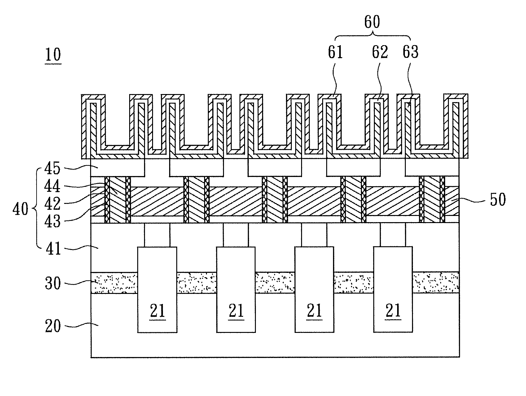
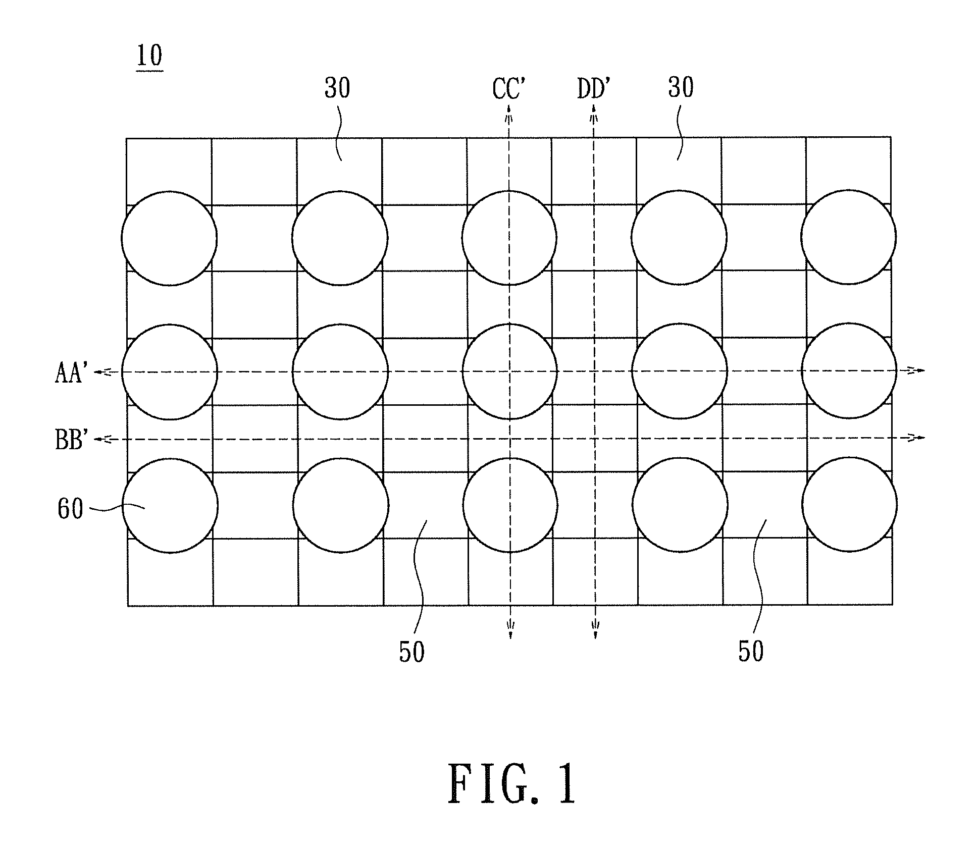
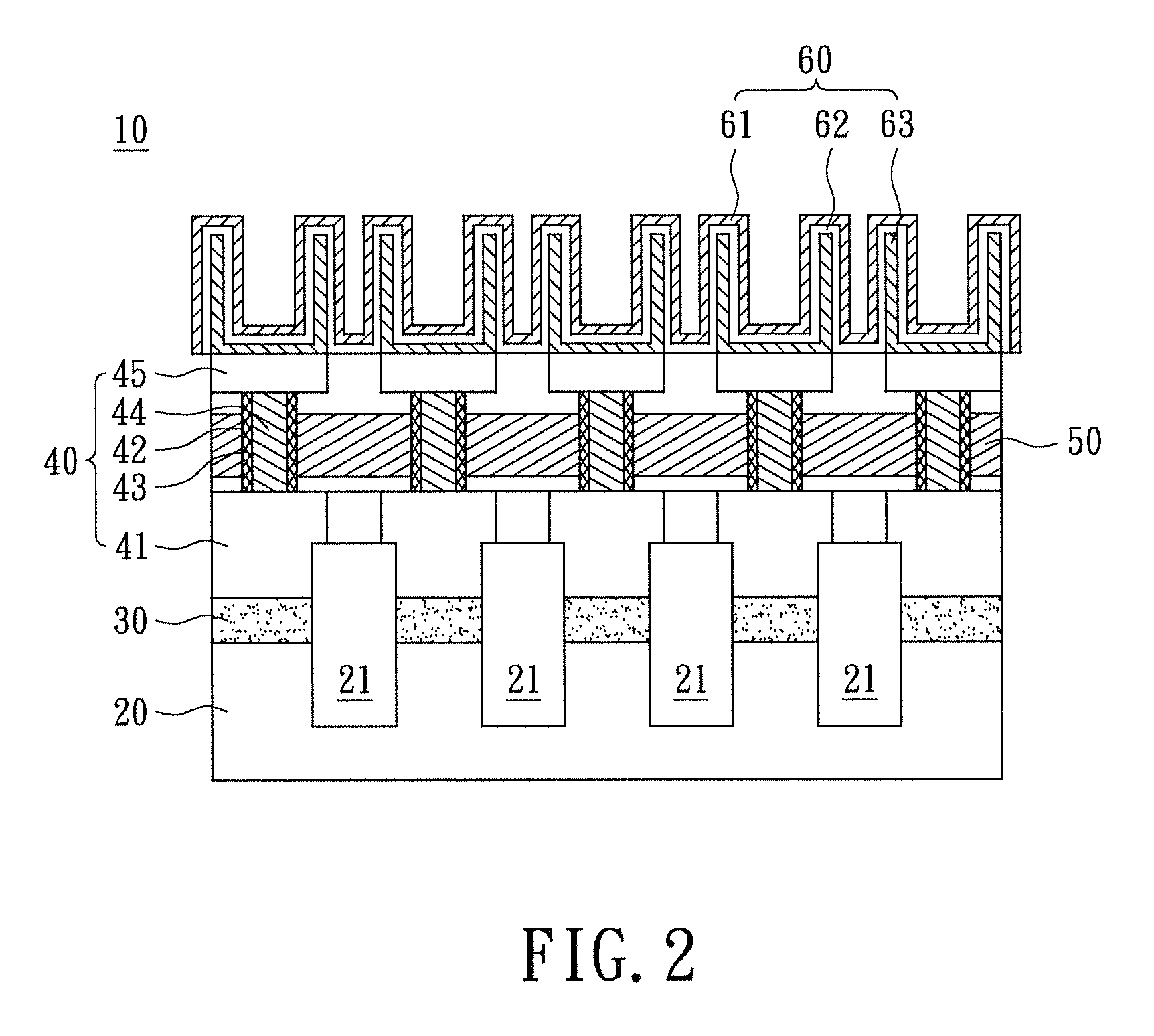
[0022]Please refer to FIG. 2, which shows a sectional view of the random access memory 10 in FIG. 1 taken along a cut-line AA′ for a first embodiment of the instant disclosure. The substrate 20 has a plurality of trenches 21 formed thereon, where the trenches 21 extend beyond the substrate 20. The trenches 21 are filled with insulating material such as silicon dioxide (silica), silicon nitride, borophosphosilicate glass (BPSG), phosphosilicate glass (PSG), undoped silicon glass (USG), or any material having high dielectric constant. However, the filler material is not restricted thereto. The bit line units 30 are arranged parallel at a distance from one another on the substrate 20. The bit line units 30 and the trenches 21 are alternately arranged on the substrate 20.

[0023]A plurality of high-k metal gate transistors 40 is disposed on the bit line units 30. Specially, the transistors 40 are perpendicular to the substrate 20, unlike the conventional ones which are parallel. Each of t...

embodiment 2

[0027]The instant disclosure further provides another high-k metal gate random access memory 10. Please refer to FIG. 6, where a sectional view of the random access memory 10 shown in FIG. 1 taken along the cut-line AA′ for the second embodiment is shown. The difference between the instant embodiment and the preceding embodiment is this: for the instant embodiment, each of the drain regions 45 and a portion of each gate structure 42 are arranged inside the respective capacitance unit 60. For this configuration, the drain regions 45 are utilized as the lower electrode layers 63 of the capacitance units 60. Then, the dielectric layer 62 and the upper electrode layer 61 are formed correspondingly on the respective drain region 45 to form the capacitance unit 60. Other physical structures of the random access memory 10 of the instant embodiment are identical to the previous embodiment, thus no further elaboration shall be provided herein.

[0028]Therefore, the metal gates 43 of the gate s...


PUM

PropertyMeasurementUnit
capacitanceaaaaaaaaaa
areaaaaaaaaaaa
sizeaaaaaaaaaa

Abstract

The instant disclosure relates to a high-k metal gate random access memory. The memory includes a substrate, a plurality of bit line units, source regions, gate structures, drain regions, word line units, and capacitance units. The substrate has a plurality of trenches, and the bit line units are arranged on the substrate. The source regions are disposed on the bit line units, and the gate structures are disposed on the source regions. Each gate structure has a metal gate and a channel area formed therein. The gate structures are topped with the drain regions. The word lines units are arranged between the source and drain regions. The capacitance units are disposed on the drain regions. Another memory is also disclosed, where each drain region and a portion of each gate structure are disposed in the respective capacitance unit, with the drain region being a lower electrode layer.

Description

BACKGROUND OF THE INVENTION[0001]1. Field of the Invention[0002]The instant disclosure relates to a random access memory; in particular, to a high-k metal gate random access memory.[0003]2. Description of Related Art[0004]In the semiconductor industry, the technology associated with dynamic random access memory (DRAM) has been advancing continuously. This technological advancement has lead to size reduction for internal semiconductor components. The size reduction means higher storage density for the memory device. Specially, the internal channel length of the semiconductor components or the gaps in between the components has a decisive impact on component density and the critical dimension. In addition, the critical dimensions of the semiconductor components are limited by the manufacturing process. Taking the existing semiconductor manufacturing process for example, the critical factor that determines the dimensions of the semiconductor components is usually the minimum resolution...

Claims


Application Information

Patent Timeline
Patent Type & Authority Patents(United States)
IPC IPC(8): H01L29/94H10B12/00
CPCH01L27/10873H01L27/10885H01L27/10891H10B12/05H10B12/488H10B12/482
Inventor LEE, TZUNG-HANHUANG, CHUNG-LINCHU, RON-FU
Owner MICRON TECH INC
Learn More