Method of generating a layout of an integrated circuit comprising both standard cells and at least one memory instance
- Summary
- Abstract
- Description
- Claims
- Application Information
AI Technical Summary
Benefits of technology
Problems solved by technology
Method used
Image
Examples
Embodiment Construction
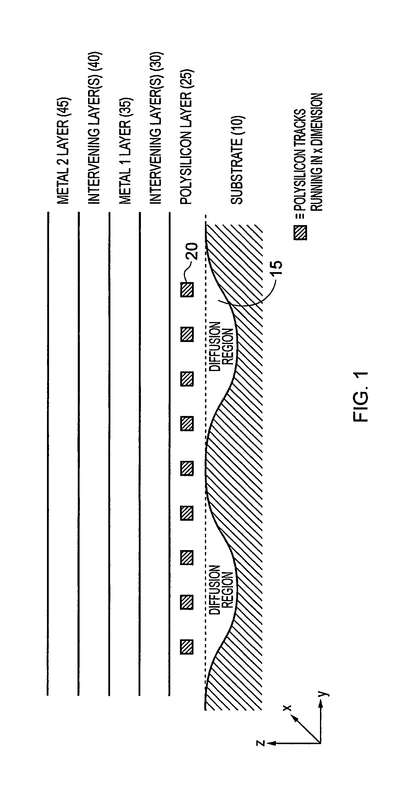
[0045]An integrated circuit may be formed of a plurality of layers established upon a substrate such as a silicon substrate, as illustrated schematically in FIG. 1. In particular, one or more diffusion regions 15 are formed in or on the substrate 10, over which a polysilicon layer 25 is provided. Within the polysilicon layer, a plurality of polysilicon tracks 20 are formed. Using the labelled dimensions of FIG. 1, these tracks run in the X direction through the polysilicon layer 25.
[0046]Above the polysilicon layer a metal one (MD layer 35 is provided, which may be separated in some embodiments from the polysilicon layer 25 by one or more intervening layers 30. In turn, the M1 layer 35 is separated from a metal two (M2) layer 45 by one or more further intervening layers 40 through which vias may be established as required. When generating a layout of an integrated circuit, the layout of each of these layers will be established. For the purposes of describing the following embodiment...
PUM
 Abstract
Description
Claims
Application Information
 - R&D
- Intellectual Property
- Life Sciences
- Materials
- Tech Scout
- Unparalleled Data Quality
- Higher Quality Content
- 60% Fewer Hallucinations
Browse by: Latest US Patents, China's latest patents, Technical Efficacy Thesaurus, Application Domain, Technology Topic, Popular Technical Reports.
© 2025 PatSnap. All rights reserved.Legal|Privacy policy|Modern Slavery Act Transparency Statement|Sitemap|About US| Contact US: help@patsnap.com


