Electrode for battery and method for manufacturing thereof

a battery and electrode technology, applied in the direction of non-aqueous electrolyte cells, cell components, conductors, etc., can solve the problems of large volume change of approximately 400%, significant structural stress on electrodes using silicon, mechanical instability, etc., to achieve long charge/discharge cycle characteristics, high efficiency characteristics, and high capacity

Inactive Publication Date: 2014-01-28
GWANGJU INST OF SCI & TECH
View PDF5 Cites 1 Cited by
  • Summary
  • Abstract
  • Description
  • Claims
  • Application Information

AI Technical Summary

Benefits of technology

[0009]Therefore, a first object of the present invention is to provide an electrode for a battery, which comprises periodically arrayed nanostructures with a desired shape formed on a silicon thin film to have long charge / discharge cycle characteristics and high capacity and high efficiency characteristics.
[0010]Moreover, a second object of the present invention is to provide a method for manufacturing an electrode for a battery, which can simply and easily form a nanopattern with nanostructures on a silicon thin film using laser interference lithography (LIL) and dry etching.

Problems solved by technology

However, despite these advantages, an electrode using silicon has the problem of large volume change of approximately 400% occurring during Li-Si alloying / dealloying.
The electrode using silicon undergoes significant structural stress due to repeated volume changes through continuous charge / discharge and thus is mechanically very unstable.
Therefore, cracks occur or part of the electrode is detached from the current collector.
In the part of the electrode detached from the current collector, lithium ions are isolated and do not participate in the electrode reaction any longer, thereby reducing the cycle performance.
However, most of the silicon nanowires or nanotubes are grown or deposited to have a non-periodic array, and thus there are structural limitations.
Moreover, the silicon nanowires or nanotubes are prepared by various bottom-up methods in which they are formed by growth from a thin film, and thus there are disadvantages to the process such as the complexity of the manufacturing process, an increase in the manufacturing process, etc.

Method used


Image

  • Electrode for battery and method for manufacturing thereof
  • Electrode for battery and method for manufacturing thereof
  • Electrode for battery and method for manufacturing thereof

Examples


examples

[0052]1. Preparation of Silicon Thin Film

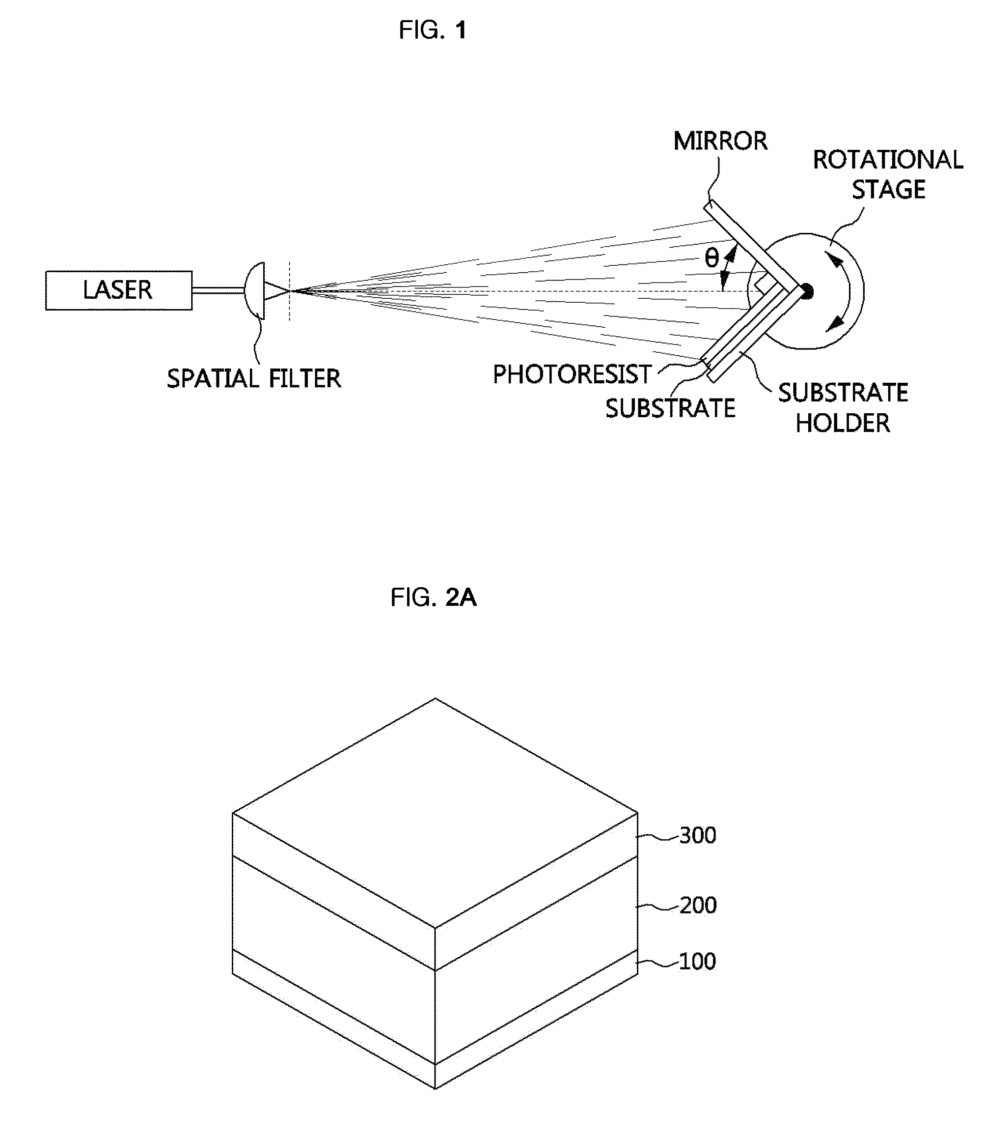
[0053]A Si thin-film with a 300 nm thickness was deposited on a substrate with a size of 1.77 cm2 using a radio-frequency (RF) magnetron sputtering method. During the sputtering, the base pressure was less than 5×10⁻⁶ Torr and the working pressure was 10 mTorr. The amount of high-purity Ar gas injected into a chamber at a predetermined pressure was fixed at 40 sccm at room temperature.

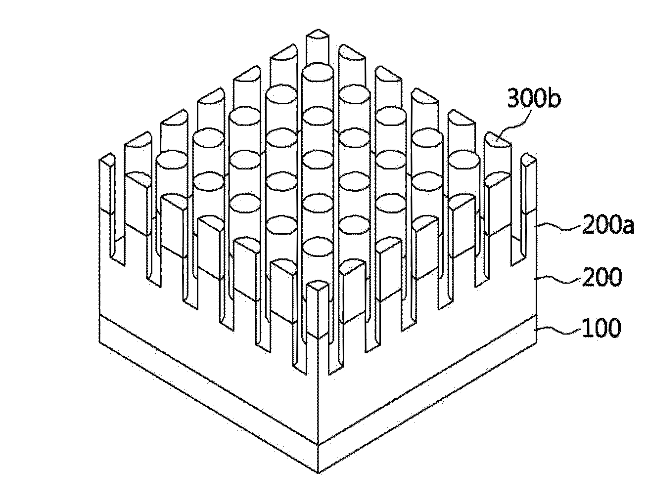
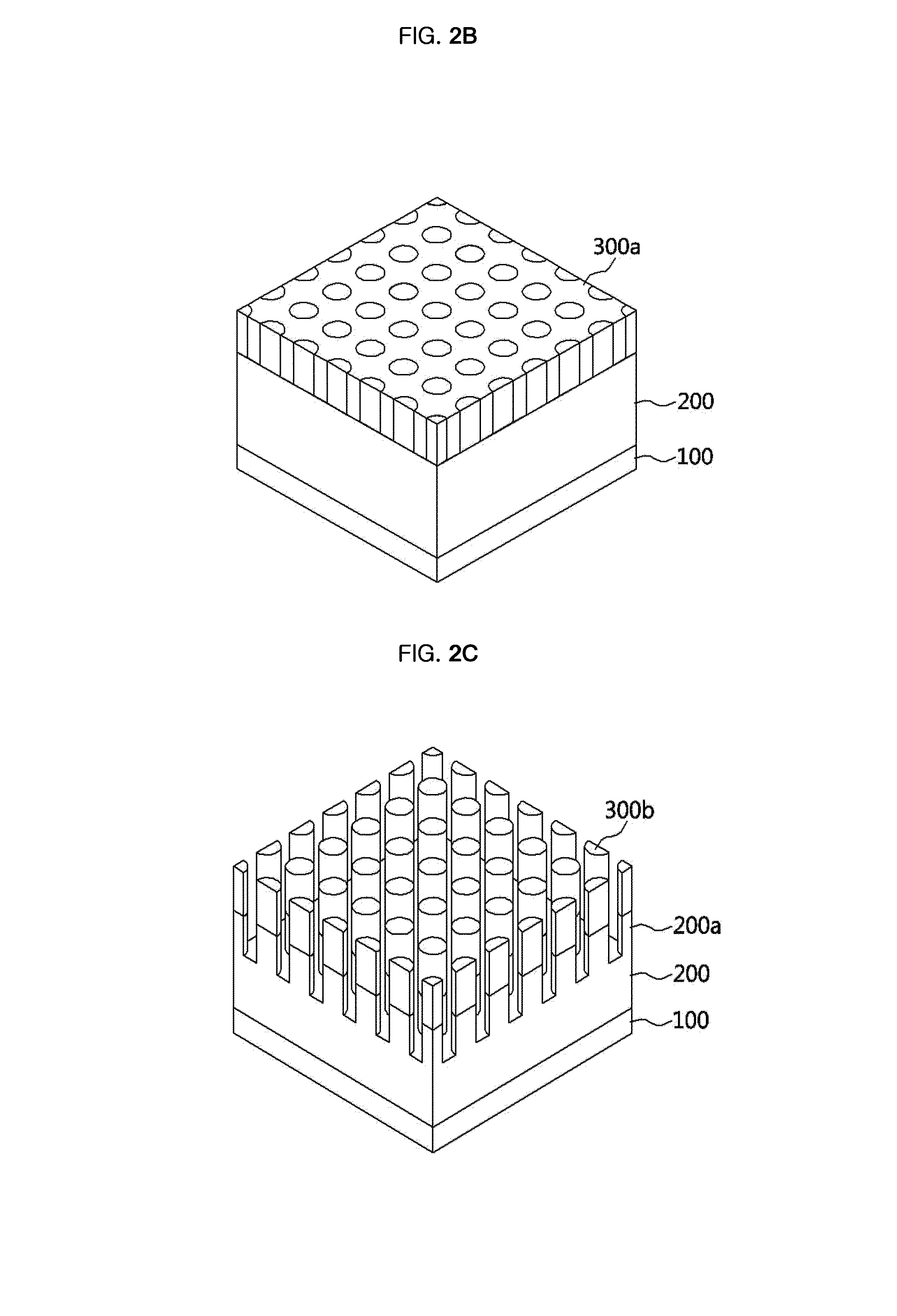
[0054]2. Formation of Nanostructures in the Form of Silicon Pillars and Silicon Wells

[0055]To form a nanopattern with a periodic array on the Si thin film, a 20 nm thick hexamethyldisilazane (HMDS, Fluka) film was first coated on the Si thin film and then annealed at 90° C. for 2 minutes. Then, a positive (+) photoresist (AZ6612, Clariant) or negative (−) photoresist (AZ6600 series, Clariant) was mixed with a thinner (AZ1512, Clariant) in a volume ratio of 1:2, and the mixture was spin-coated on the HMDS film, thereby forming a photoresist layer. Subsequently, a...


PUM

PropertyMeasurementUnit
distanceaaaaaaaaaa
diameteraaaaaaaaaa
depthaaaaaaaaaa

Abstract

An electrode for a battery and a method for manufacturing the same are disclosed. The electrode for a battery according to the present invention comprising silicon nanostructures integrally formed on a silicon thin film and having a period array can reduce the internal resistance, have better charge transport properties, and reduce the structural stress, thereby exhibiting high storage capacity, high efficiency charge / discharge characteristics, and long charge / discharge cycle characteristics. Moreover, the method for manufacturing the electrode for a battery according to the present invention can simply and easily form a nanopattern with nanostructures on a silicon thin film using laser interference lithography (LIL) and dry etching.

Description

CROSS-REFERENCE TO RELATED APPLICATION[0001]This application claims priority under 35 U.S.C. §119(e) to U.S. Patent Application No. 61 / 526,928 filed on Aug. 24, 2011, which is herein incorporated by reference in its entirety.BACKGROUND OF THE INVENTION[0002]1. Field of the Invention[0003]The present invention relates to an electrode for a battery and a method for manufacturing thereof and, more particularly, to a silicon electrode for a battery, which comprises periodically arrayed nanostructures that contribute to the improvement of battery life and capacity, and a method for manufacturing thereof, which can simply and easily form a nanopattern with nanostructures on a silicon thin film using laser interference lithography (LIL) and dry etching.[0004]2. Description of the Related Art[0005]As the use of portable electronic devices has increased due to the development of science and technology, the demand for secondary batteries which can be used through repeated charging and dischar...

Claims


Application Information

Patent Timeline
Patent Type & Authority Patents(United States)
IPC IPC(8): H01M4/00
CPCH01B1/122B82Y30/00H01M4/386H01M4/0492H01M10/052Y02E60/12Y02E60/10H01M4/134G03F7/20H01M4/1395B82B3/00
Inventor KIM, WON-BAEJUNG, GUN-YOUNGNAM, SANG-HOONKIM, KI-SEOK
Owner GWANGJU INST OF SCI & TECH
Why Eureka
Try Eureka