Composition for removing a photoresist and method of manufacturing a thin-film transistor substrate using the composition

a thin-film transistor and composition technology, applied in the field of composition for removing a photoresist and a thin-film transistor substrate, can solve the problems of corroding output electrodes, difficult to uniformly form organic layers on the entire surface of tft substrates, undesirable thick organic layers, etc., to reduce the rework process of organic layers, and improve the removing ability of organic layers

Active Publication Date: 2013-12-10
SAMSUNG DISPLAY CO LTD
View PDF5 Cites 16 Cited by
  • Summary
  • Abstract
  • Description
  • Claims
  • Application Information

AI Technical Summary

Benefits of technology

[0009]Example embodiments provide a composition for removing a photoresist capable of reducing corrosion of a metal layer and improving a removing ability of a photosensitive organic pattern.
[0022]The corrosion of a lower metal layer disposed under an organic layer, e.g., as a planarizing layer, or a photoresist pattern, e.g., as an etch-stopping layer, may be reduced to improve a removing ability of the organic layer and the photoresist pattern. Thus, a reliability of a rework process of the organic layer may be improved, and a removing time of the organic layer and the photoresist pattern may be decreased.
[0023]Also, when the organic layer or the photoresist pattern is formed using a positive or a negative photoresist composition, the organic layer and the photoresist pattern may be easily removed by the composition for removing a photoresist. Therefore, the rework process or the removing process of the photoresist pattern may be performed using a single stripping device regardless of a type of the photoresist composition to improve a productivity of a TFT substrate.

Problems solved by technology

When an inorganic layer including an inorganic material is formed on the TFT substrate, the inorganic layer may be undesirably thick.
However, uniformly forming the organic layer on an entire surface of the TFT substrate is difficult, and thus a rework process is performed in order to provide an organic layer having suitable surface characteristics.
In addition, the output electrode may be corroded by a stripping composition for removing the organic layer, decreasing desirable characteristics of the thin-film transistor because the output electrode is already exposed through the contact hole in removing the organic layer.
However, the stripper including the amine compound is limited in its ability to remove the photoresist pattern, depending on the type of the photoresist composition, and the stripper undesirably corrodes metal.

Method used


Image

  • Composition for removing a photoresist and method of manufacturing a thin-film transistor substrate using the composition
  • Composition for removing a photoresist and method of manufacturing a thin-film transistor substrate using the composition
  • Composition for removing a photoresist and method of manufacturing a thin-film transistor substrate using the composition

Examples


example 1

[0112]Based on a total weight of a composition for removing a photoresist, about 5% by weight of tetramethyl ammonium hydroxide (“TMAH”), about 59.9% by weight of dimethylene glycol monomethyl ether (“MDG”), about 5% by weight of an alkanol amine, about 0.1% by weight of tolytriazole, and about 10% by weight of deionized (“DI”) water were mixed to prepare the composition for removing the photoresist according to Example 1 of the present invention.

[0113]Compositions for removing a photoresist according to Example 2 and 3 including the foregoing components and in the amounts shown in Table 1 were prepared via substantially the same method as preparing the composition for removing the photoresist according to Example 1.

[0114]

TABLE 1ComponentExample 2Example 3TMAHabout 4.0% by weightabout 3.0 by weightMDGabout 50.9% by weightabout 51.9% by weightNMPabout 30.0% by weightabout 25.0% by weightalkanol amineabout 5.0% by weightabout 5.0% by weighttolytriazoleabout 0.1% by weightabout 0.1% by...

experiment 1

Evaluation of Removing Ability of an Organic Layer

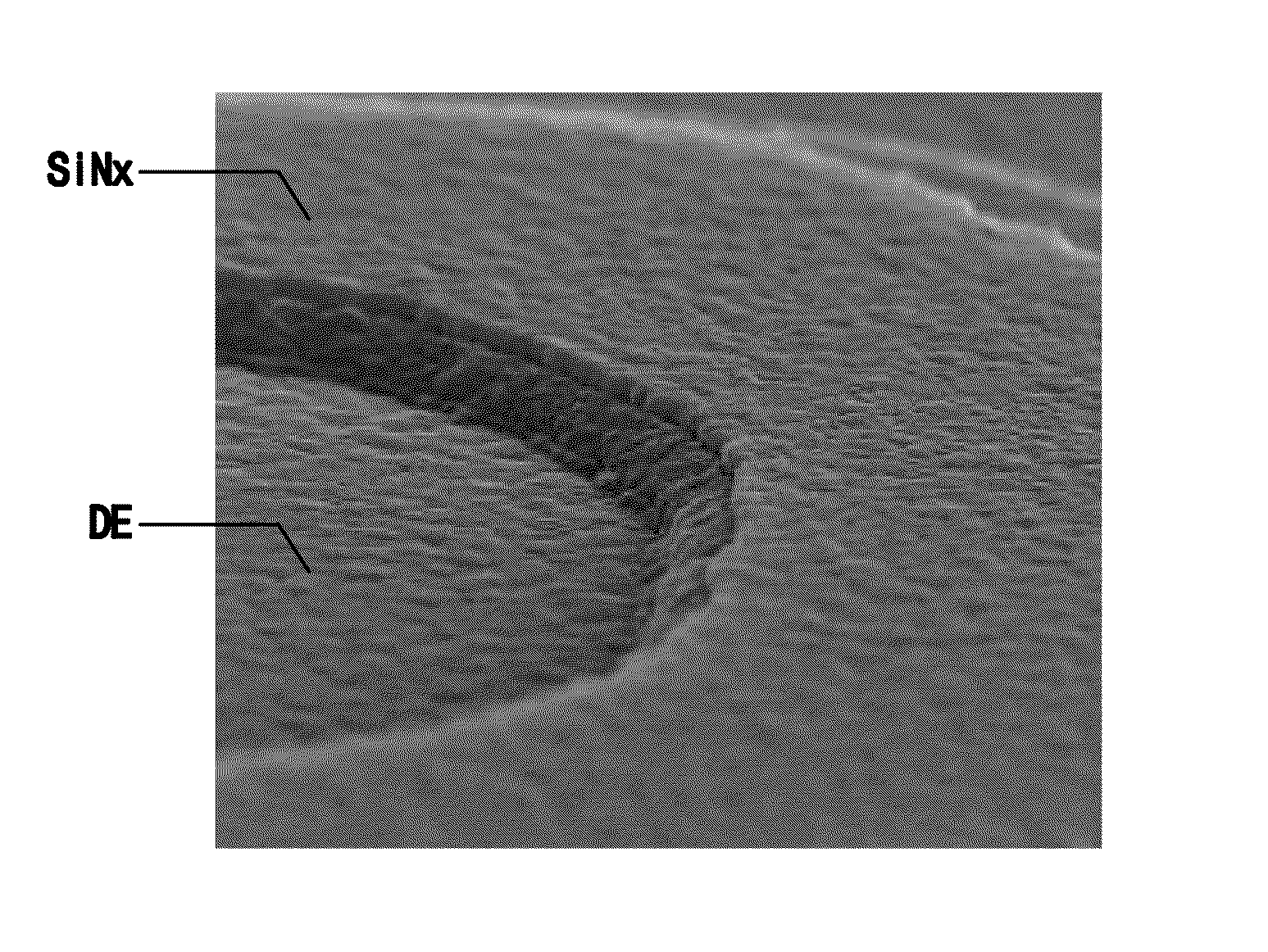
[0121]The organic layer was removed using the composition for removing the photoresist according to Example 1 maintained in a temperature of about 50° C. in each of Substrate Sample 1 to Substrate Sample 6. The contact region removing the organic layer in each of the Substrate Sample 1 to Substrate Sample 6 was imaged using the scanning electrode microscope, and the SEMs are provided in FIGS. 9B and 10B.

[0122]For each of Substrate Samples 2 and 7, the organic layer was removed using the composition for removing the photoresist according to Example 2 maintained in a temperature of about 50° C.

[0123]For each of Substrate Sample 3 and 8, the organic layer was removed using the composition for removing the photoresist according to Example 3 maintained in a temperature of about 50° C.

[0124]For each of Substrate Sample 4 and 9, the organic layer was removed using the composition for removing the photoresist according to Comparative Example...

experiment 2

Evaluation of Corroding a Metal Layer

[0138]The composition for removing the photoresist according to Example 1 was provided to each of Metal Sample 1 and 6 for about 10 minutes. The composition for removing the photoresist according to Example 2 was provided to each of Metal Sample 2 and 7, and the composition for removing the photoresist according to Example 3 was provided to each of Metal Sample 3 and 8 for about 10 minutes.

[0139]In addition, the composition for removing the photoresist according to Comparative Example 1 was provided to each of Metal Samples 4 and 9, and the composition for removing the photoresist according to Comparative Example 2 was provided to each of Metal Samples 5 and 10 for about 10 minutes.

[0140]In each of Metal Samples 1 to 10, the corrosion of the aluminum pattern or the copper pattern was observable with the naked eye of a viewer. The obtained results are illustrated in Table 4. In Table 4, “∘” represents when the aluminum pattern or the copper patter...


PUM


Abstract

A composition for removing a photoresist, the composition including about 1% by weight to about 10% by weight of tetramethyl ammonium hydroxide (“TMAH”), about 1% by weight to about 10% by weight of an alkanol amine, about 50% by weight to about 70% by weight of a glycol ether compound, about 0.01% by weight to about 1% by weight of a triazole compound, about 20% by weight to about 40% by weight of a polar solvent, and water, each based on a total weight of the composition.

Description

PRIORITY STATEMENT[0001]This application claims priority to Korean Patent Application No. 2011-70014, filed on Jul. 14, 2011, and all the benefits accruing therefrom under 35 U.S.C. §119, the content of which in its entirety is herein incorporated by reference.BACKGROUND OF THE INVENTION[0002]1. Field of the Invention[0003]This disclosure relates to a composition for removing a photoresist and a method of manufacturing a thin-film transistor substrate using the composition. More particularly, this disclosure relates to a composition for removing a photoresist which can be used in the manufacture of a thin-film transistor substrate, and a method of manufacturing a thin-film transistor substrate using the composition.[0004]2. Description of the Related Art[0005]Generally, a thin-film transistor substrate (“TFT substrate”) includes a thin-film transistor, an insulating layer protecting the thin-film transistor, and a pixel electrode electrically connected to the thin film transistor. T...

Claims


Application Information

Patent Timeline
Patent Type & Authority Patents(United States)
IPC IPC(8): H01L21/312
CPCG03F7/425H01L21/31133H01L29/66765H01L27/1288G03F7/0395H01L21/0274
Inventor KIM, BONG-KYUNCHOI, SHIN-ILPARK, HONG-SICKLEE, WANG-WOOJANG, SEOK-JUNKIM, BYUNG-UKPARK, SUN-JOOYOON, SUK-ILJEONG, JONG-HYUNHUR, SOON-BEOM
Owner SAMSUNG DISPLAY CO LTD
Why Eureka
Try Eureka