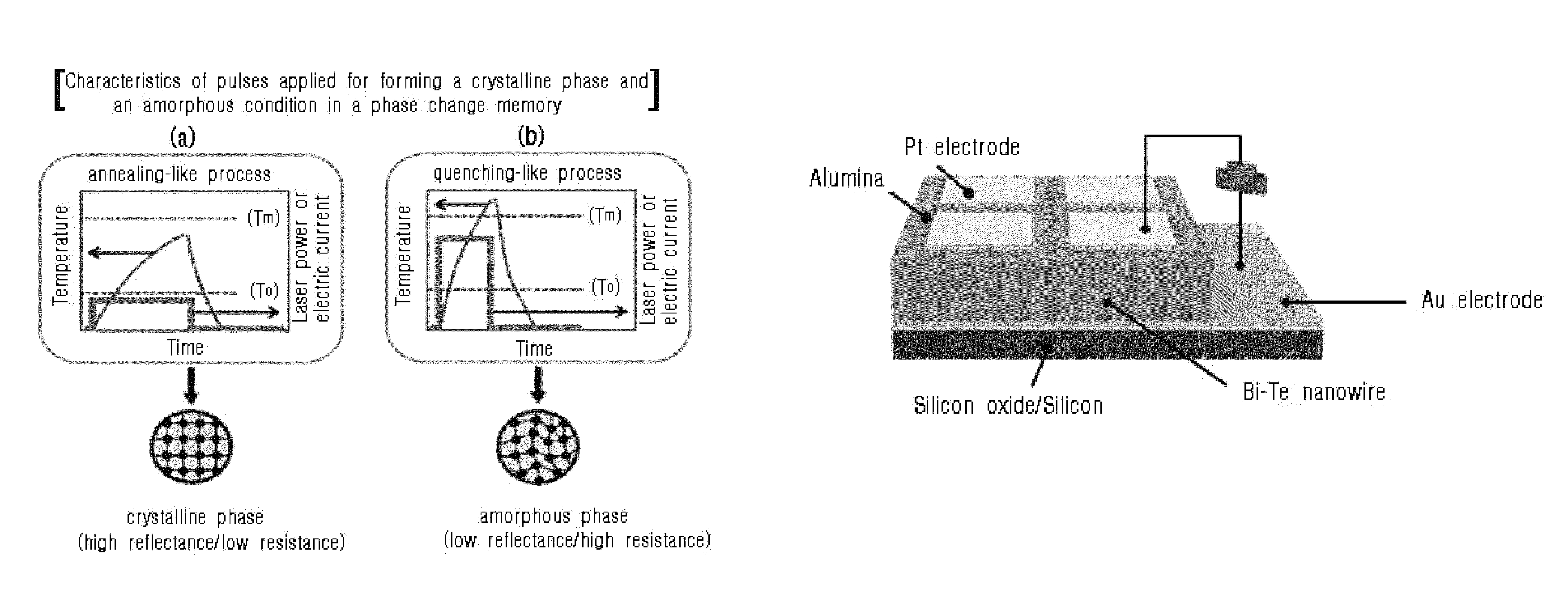
Phase change memory device comprising bismuth-tellurium nanowires
a memory device and phase change technology, applied in semiconductor devices, digital storage, instruments, etc., can solve the problems of high production cost per unit, complex preparation process, and inability to control the composition ratio of said elements, so as to reduce the unit cost of production and facilitate and prompt production
- Summary
- Abstract
- Description
- Claims
- Application Information
AI Technical Summary
Benefits of technology
Problems solved by technology
Method used
Image

Examples
example 1
Preparation of Phase Change Memory Device
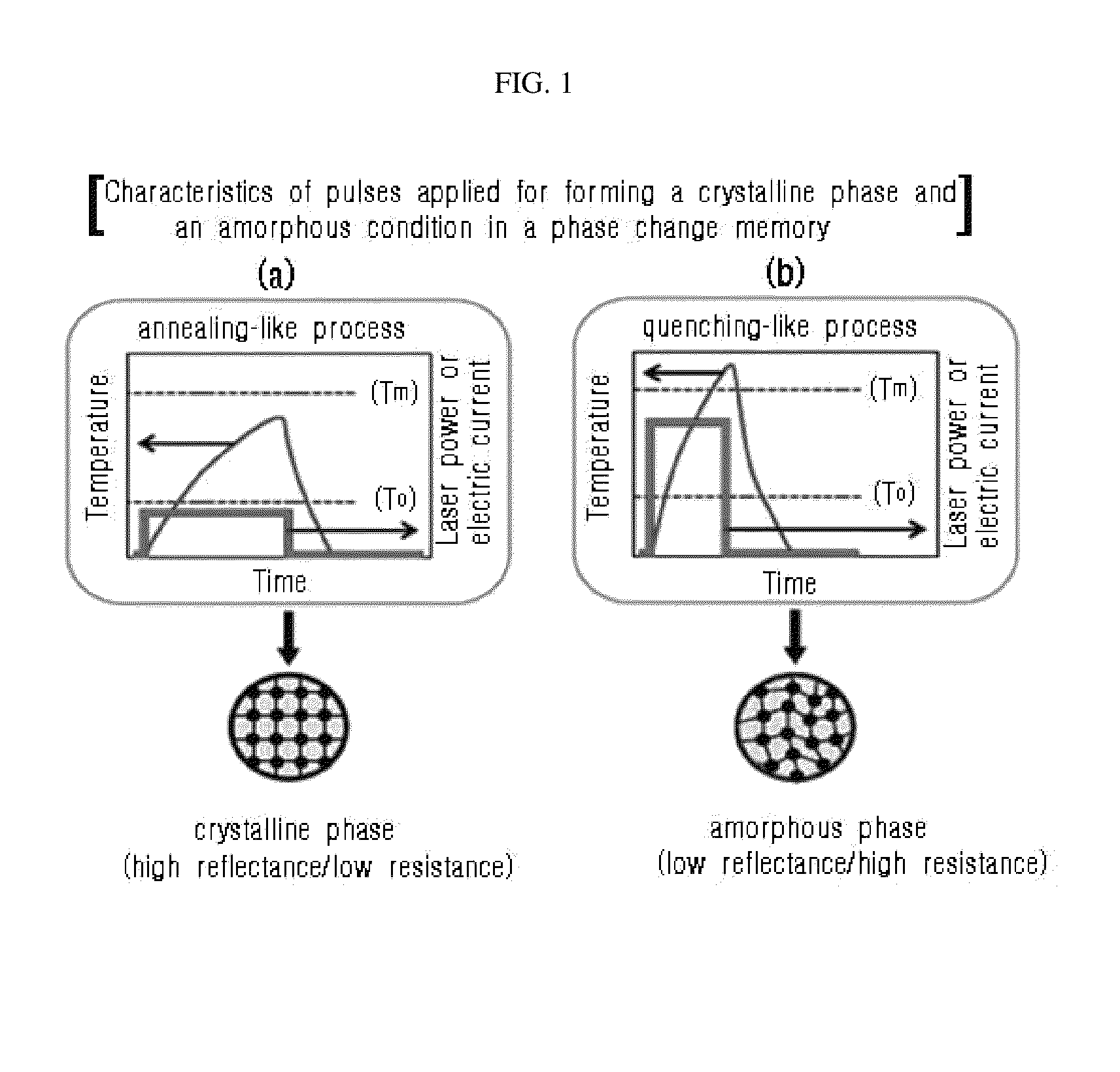
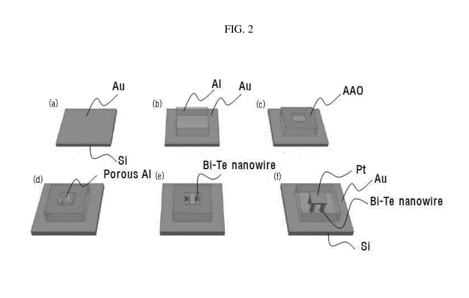
[0075]With reference to a schematic view of FIG. 2, a process of preparing a phase change memory device is explained below.
[0076]First, a metal electrode to be used as a bottom electrode, such as Au and Pt, was deposited on a silicon substrate (FIG. 2a).
[0077]On the electrode, Al with a thickness of about 1 μm was patterned by means of a lithography method and a lift-off method, and then deposited (FIG. 2b).
[0078]Then, the other part was passivated with a resist, such that only a part to form AAO can be exposed to an electrolyte solution, followed by anodization (FIG. 2c, d).
[0079]With reference to FIG. 3, the method of anodizing Al is amplified below (FIG. 2c, d).
[0080]Oxalic acid (C2H2O4, 0.3 M) was used as an electrolyte for anodization, wherein the temperature was maintained at 15° C. and a voltage of 40 V was applied.
[0081]First, when the AAO layer formed after carrying out the first anodization for about 2 minutes was dissolved in a mix...
experimental example 1
Investigation of Bi2Te3 Characteristics
[0089]FIG. 7 being a result of measuring X-ray diffraction of Bi2Te3 prepared in the above example 1 represented a polycrystalline structure, wherein a main peak in a direction (110) and peaks in other directions are present.
[0090]In addition, as a result of observation for microstructures using a transmission electron microscope, the diffraction patterns (inside of FIG. 8(a)) were identical to the results of measuring X-ray diffraction as well as the crystalline structure was observed as shown in FIG. 8(a).
[0091]The phase of Bi2Te3 nanowires was changed depending on temperature, and thus, for identifying change of resistance value, temperature dependency of resistance was measured.
[0092]As shown in FIG. 9, as temperature increased, the resistance value was slightly reduced, because the initial phase nanowires were a crystalline phase. However, the resistance value rapidly increased at about 231° C., and the condition of high resistance was mai...
PUM
| Property | Measurement | Unit |
|---|---|---|
| diameter | aaaaa | aaaaa |
| thickness | aaaaa | aaaaa |
| pore size | aaaaa | aaaaa |
Abstract
Description
Claims
Application Information
 - R&D
- Intellectual Property
- Life Sciences
- Materials
- Tech Scout
- Unparalleled Data Quality
- Higher Quality Content
- 60% Fewer Hallucinations
Browse by: Latest US Patents, China's latest patents, Technical Efficacy Thesaurus, Application Domain, Technology Topic, Popular Technical Reports.
© 2025 PatSnap. All rights reserved.Legal|Privacy policy|Modern Slavery Act Transparency Statement|Sitemap|About US| Contact US: help@patsnap.com