Formation of photovoltaic absorber layers on foil substrates

a technology of absorber layer and foil, which is applied in the direction of sustainable manufacturing/processing, final product manufacturing, coatings, etc., can solve the problems of damage to the substrate upon which deposition occurs, damage to the substrate, and damage to the substra

Inactive Publication Date: 2013-09-24
AERIS CAPITAL SUSTAINABLE IP
View PDF63 Cites 1 Cited by
  • Summary
  • Abstract
  • Description
  • Claims
  • Application Information

AI Technical Summary

Benefits of technology

The patent describes a method for processing a flexible metal substrate coated with a nascent absorber layer. The method involves continuously passing the substrate through a furnace in a non-oxygen group VIA vapor atmosphere to incorporate the group VIA element into the absorber layer without damaging or destroying the metal substrate and without generating substantial hydrogen selenide. The processing can occur in stages, with at least one stage occurring in a non-oxygen group VIA vapor and the substrate spending a total time above ambient temperature in such vapor. This method allows for the effective and controlled processing of flexible metal substrates with nascent absorber layers.

Problems solved by technology

Unfortunately, current techniques for depositing CIGS absorber layers are incompatible with the use of aluminum foil as a substrate.
These deposition processes are typically carried out at high temperatures and for extended times. Both factors can result in damage to the substrate upon which deposition is occurring.
Such damage can arise directly from changes in the substrate material upon exposure to heat, and / or from undesirable chemical reactions driven by the heat of the deposition process.
These limitations have excluded the use of aluminum and aluminum-foil based foils.
Advantages to this deposition approach include both the relatively lower deposition temperature and the rapidity of the deposition process.
While use of aluminum (Al) as a substrate for solar cell devices would be desirable due to both the low cost and lightweight nature of such a substrate, conventional techniques that effectively anneal the CIGS absorber layer also heat the substrate to high temperatures, resulting in damage to Al substrates.
There are several factors that result in Al substrate degradation upon extended exposure to heat and / or selenium-containing compounds for extended times. First, upon extended heating, the discrete layers within a Mo-coated Al substrate can fuse and form an intermetallic back contact for the device, which decreases the intended electronic functionality of the Mo-layer.
Second, the interfacial morphology of the Mo layer is altered during heating, which can negatively affect subsequent CIGS grain growth through changes in the nucleation patterns that arise on the Mo layer surface.
Third, upon extended heating, Al can migrate into the CIGS absorber layer, disrupting the function of the semiconductor.
Fourth, the impurities that are typically present in the Al foil (e.g. Si, Fe, Mn, Ti, Zn, and V) can travel along with mobile Al that diffuses into the solar cell upon extended heating, which can disrupt both the electronic and optoelectronic function of the cell.
Fifth, when Se is exposed to Al for relatively long times and at relatively high temperatures, aluminum selenide can form, which is unstable.
Hydrogen selenide is a highly toxic gas, whose free formation can pose a safety hazard.
For all these reasons, high-temperature deposition, annealing, and selenization are therefore impractical for substrates made of aluminum or aluminum alloys.
Because of the high-temperature, long-duration deposition and annealing steps, CIGS solar cells cannot be effectively fabricated on aluminum substrates (e.g. flexible foils comprised of Al and / or Al-based alloys) and instead must be fabricated on heavier substrates made of more robust (and more expensive) materials, such as stainless steel, titanium, or molybdenum foils, glass substrates, or metal- or metal-oxide coated glass.
Thus, even though CIGS solar cells based on aluminum foils would be more lightweight, flexible, and inexpensive than stainless steel, titanium, or molybdenum foils, glass substrates, or metal- or metal-oxide coated glass substrates, current practice does not permit aluminum foil to be used as a substrate.

Method used


Image

  • Formation of photovoltaic absorber layers on foil substrates
  • Formation of photovoltaic absorber layers on foil substrates

Examples


Embodiment Construction

[0018]Although the following detailed description contains many specific details for the purposes of illustration, anyone of ordinary skill in the art will appreciate that many variations and alterations to the following details are within the scope of the invention. Accordingly, the exemplary embodiments of the invention described below are set forth without any loss of generality to, and without imposing limitations upon, the claimed invention.

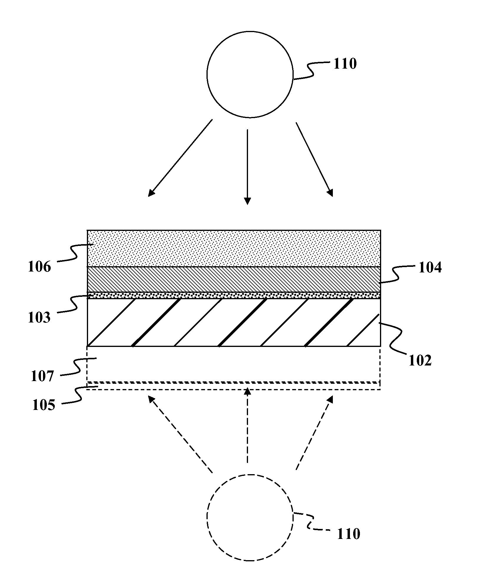
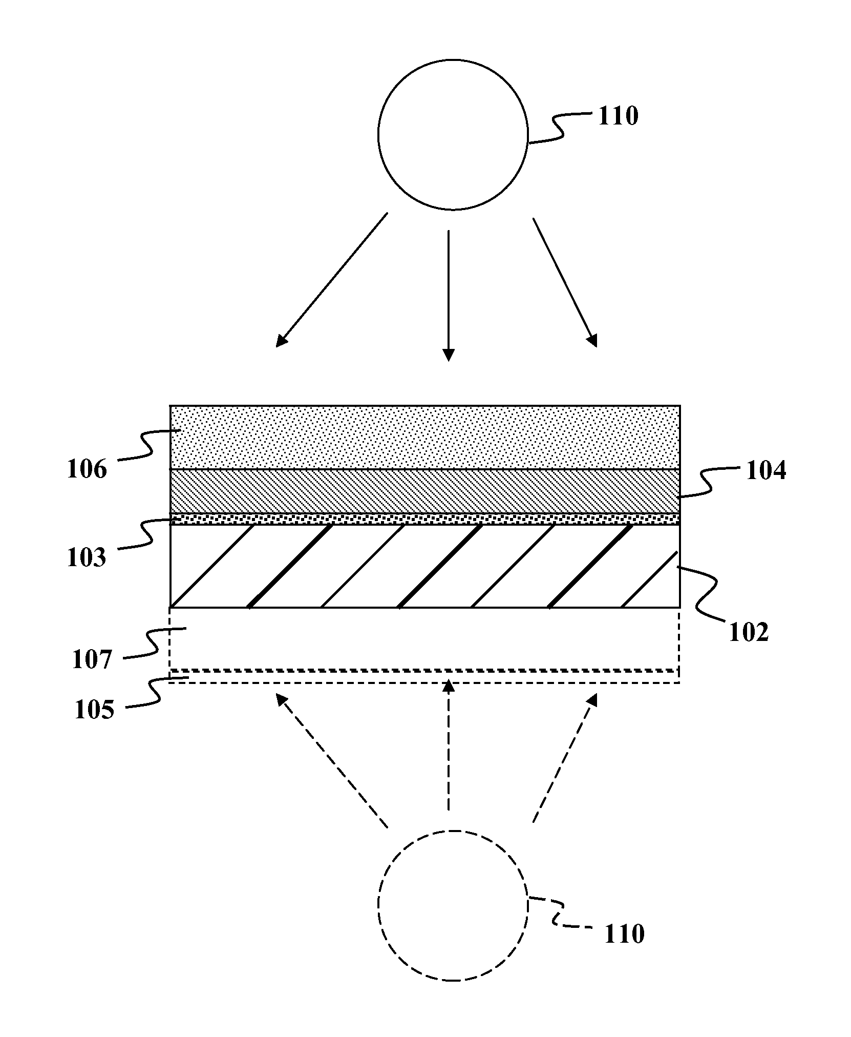
[0019]Embodiments of the present invention allow fabrication of CIGS absorber layers on aluminum foil substrates. The invention lends itself to several variants (which remain, however, optional) used as alternatives or in combination. According to embodiments of the present invention, a nascent absorber layer containing elements of group IB and IIIA formed on an aluminum substrate by solution deposition may be annealed by rapid heating from an ambient temperature to a plateau temperature range of between about 200° C. and about 600° C. The t...


PUM


Abstract

An absorber layer of a photovoltaic device may be formed on an aluminum or metallized polymer foil substrate. A nascent absorber layer containing one or more elements of group IB and one or more elements of group IIIA is formed on the substrate. The nascent absorber layer and / or substrate is then rapidly heated from an ambient temperature to an average plateau temperature range of between about 200° C. and about 600° C. and maintained in the average plateau temperature range 1 to 30 minutes after which the temperature is reduced.

Description

CROSS-REFERENCE TO RELATED APPLICATION[0001]This application is a continuation-in-part of U.S. patent application Ser. No. 12 / 060,221 filed Mar. 31, 2008 which claims the benefit of priority to U.S. Provisional Application Ser. No. 60 / 909,357 filed Mar. 30, 2007 and U.S. Provisional Application Ser. No. 60 / 911,259 filed Apr. 11, 2007. This application is a continuation-in-part of U.S. patent application Ser. No. 10 / 943,685 filed Sep. 18, 2004. The entire disclosures of all the foregoing applications are fully incorporated herein by reference for all purposes.FIELD OF THE INVENTION[0002]The present invention relates to fabrication of photovoltaic devices and more specifically to processing and annealing of absorber layers for photovoltaic devices.BACKGROUND OF THE INVENTION[0003]Efficient photovoltaic devices, such as solar cells, have been fabricated using absorber layers made with alloys containing elements of group IB, IIIA and VIA, e.g., alloys of copper with indium and / or galliu...

Claims


Application Information

Patent Timeline
IPC IPC(8): B05D5/12H01L21/00H01L21/06H01L27/14H01L31/00
CPCH01L31/1864H01L31/0322H01L31/0392H01L31/03928H01L21/02422H01L21/02425H01L21/02491H01L21/02568H01L21/02601H01L21/02614H01L21/02628Y02E10/541H01L31/03923H01L31/03925H01L31/03926Y02P70/50
Inventor LEIDHOLM, CRAIGBOLLMAN, BRENT
Owner AERIS CAPITAL SUSTAINABLE IP
Why Eureka
Try Eureka