Silicon wafer and method for producing the same

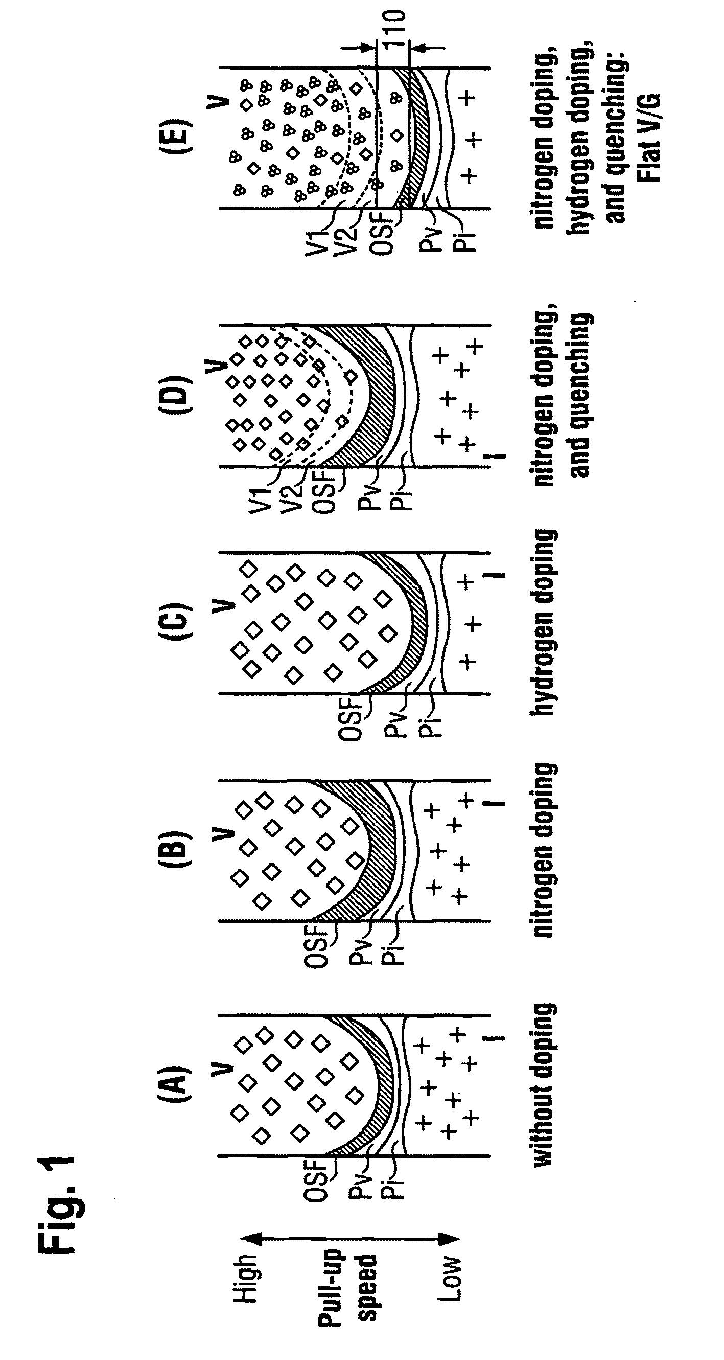
a technology of silicon wafers and silicon ions, applied in the direction of polycrystalline material growth, crystal growth process, polycrystalline material growth, etc., can solve the problem that the voltage resistance characteristics of nitrogen doped crystal obtained by jp 3255114 cannot be said to have high c-mode characteristics completely, and the voltage resistance characteristics of oxide films are deteriorated, so as to achieve high c-mode pass rate, excellent voltage characteristics, and high c-mode characteristics

Active Publication Date: 2013-09-03
SILTRONIC AG
View PDF12 Cites 0 Cited by
  • Summary
  • Abstract
  • Description
  • Claims
  • Application Information

AI Technical Summary

Benefits of technology

[0010]With this background, it is an object of the present invention to provide a silicon wafer composed of a silicon crystal displaying excellent voltage characteristics with respect to an oxidized film, and high C-mode characteristics (good in high C-mode pass rate). In addition, it is another object of the present invention to provide a method for producing the aforesaid silicon wafer. In view of the above problems, as a result of intensive studies carried out by the present inventors, it has been found that a silicon crystal (single crystal silicon) having excellent voltage resistance characteristics with respect to an oxidized film, and high C-mode characteristics (good in high C-mode pass rate) can be obtained by the addition of nitrogen and hydrogen in predetermined concentration, along with a “quenching” treatment carried out at predetermined temperature gradient in pulling-up the silicon crystal (hereafter referred to as “average temperature gradient in a crystal growth longitudinal direction” or simply “G”), and at predetermined pulling speed (hereafter referred to simply as “V”). It has been found that, by this treatment, a silicon crystal having improved voltage resistance characteristics with respect to an oxidized film, and improved C-mode characteristics, can be obtained.

Problems solved by technology
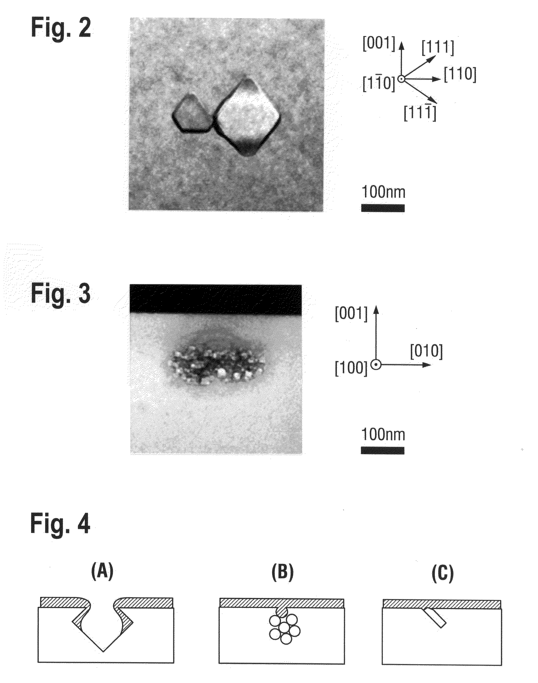
In such a wafer, grown-in defects generated by aggregation of point defects during crystal growth are present.
Exposure of these defects at the wafer surface has raised a problem, due to deterioration of the characteristics of a device formed thereon.
However, such an OSF region has a low index showing absence of a crystal defects, which deteriorates the voltage resistance characteristics of an oxide film, that is, C-mode (a true destruction region) characteristics (high C-mode pass rate).
In conclusion, the nitrogen doped crystal obtained by JP 3255114 cannot be said to have high C-mode characteristics totally, and is inferior in voltage resistance characteristics of an oxide film.
This means that voids or some kind of microdefects are present over all of the aforesaid nitrogen doped crystal, which renders the wafers unsuitable for use in fabricating semiconductor devices.

Method used


Image

  • Silicon wafer and method for producing the same
  • Silicon wafer and method for producing the same
  • Silicon wafer and method for producing the same

Examples


example 1

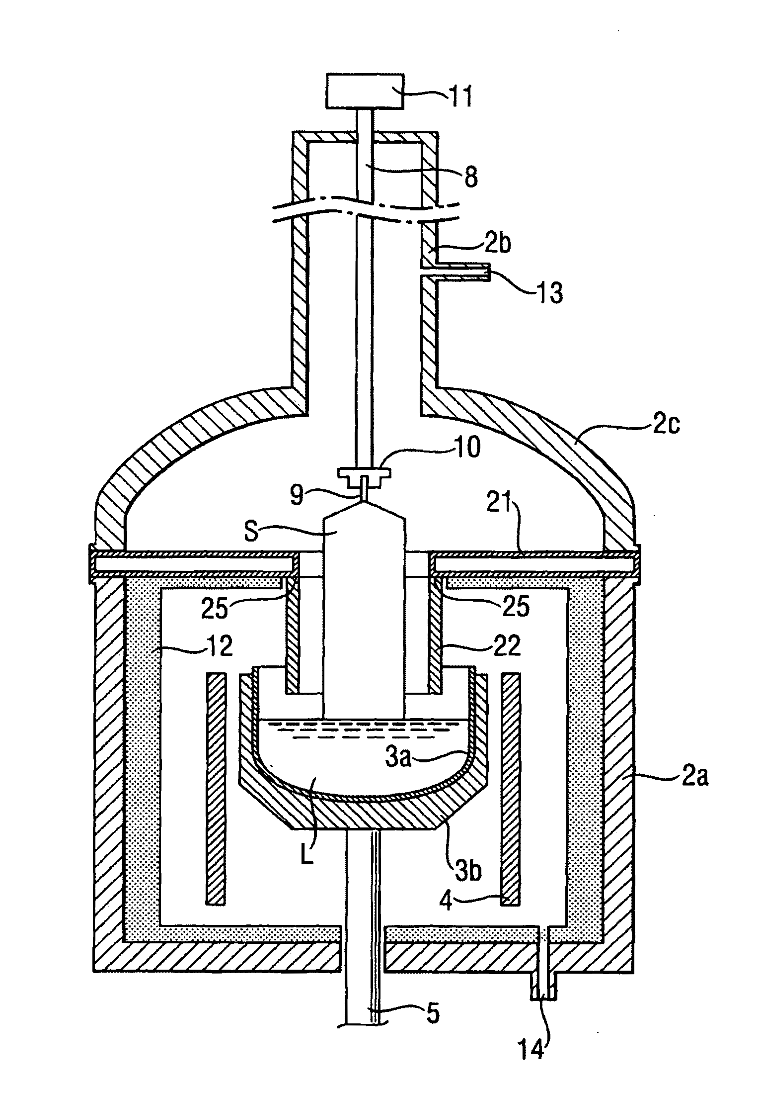
[0090]Pulling of a silicon single crystal was carried out by using a silicon crystal production apparatus. The silicon crystal production apparatus used in the present example is a single crystal production apparatus having the cooling structure 22 shown in FIG. 5. Such an apparatus is used in producing a silicon crystal by the usual CZ method. In using the above apparatus, the crucible diameter was 22 inch, the semiconductor charge inserted into the crucible was 100 kg, and growing single crystal S was an 8 inch crystal.

[0091]As a material for the cooling structure 22, silver was used, and the cooling structure 22 had an inner diameter of 260 mm, an outer diameter of 300 mm, and a length of 280 mm. As the liquid cooling structure 21, a constitution of a doughnut-shaped water cooling chamber having a cooling water passage inside was used, and the liquid cooling structure 21 was attached at the lower part of the middle chamber 2c.

[0092]Specifically, the aforesaid production apparatu...

example 2

[0106]A silicon single crystal was pulled similarly as in Example 1, except that conditions of oxygen concentration, pulling speed, along with minimal value and maximal value of V / G were set as described in Table 3.

example 3

[0107]A silicon single crystal was pulled similarly as in Example 1, except that conditions of oxygen concentration, pulling speed, along with minimal value and maximal value of V / G were set as described in Table 3.


PUM

PropertyMeasurementUnit
pressureaaaaaaaaaa
temperatureaaaaaaaaaa

Abstract

Silicon wafers having excellent voltage resistance characteristics of an oxide film and high C-mode characteristics are derived from single crystal silicon ingots doped with nitrogen and hydrogen, characterized in that a plurality of voids constituting a bubble-like void aggregates are present ≧50% relative to total voids; a V1 region having a void density of over 2×10⁴ / cm3 and below 1×10⁵ / cm3 is ≦20% of the total area of wafer; a V2 region having a void density of 5×10² to 2×10⁴ / cm3 occupies ≧80% of the total area of the wafer; and bulk microdefect density is ≧5×10⁸ / cm3.

Description

CROSS-REFERENCE TO RELATED APPLICATIONS[0001]This application claims priority to Japanese Patent Application Nos. 2008-334755 filed Dec. 26, 2008 and 2009-194085 filed Aug. 25, 2009 which are herein incorporated by reference.BACKGROUND OF THE INVENTION[0002]1. Field of the Invention[0003]The present invention relates to a silicon wafer and a method for producing the same. More specifically, the present invention relates to a silicon wafer (mirror surface wafer) obtained by doping nitrogen and hydrogen, and polishing (mirror fabrication) having a void region, and a method for producing the same.[0004]2. Background Art[0005]A silicon wafer used as a substrate for semiconductor integrated circuits (a semiconductor device) is cut from a silicon crystal, and the most widely adopted method for producing this single crystal is growth by the Czochralski method (hereafter referred to also the “CZ method”). The CZ method is a method for growing a single crystal by contacting a seed crystal wi...

Claims


Application Information

Patent Timeline
Patent Type & Authority Patents(United States)
IPC IPC(8): C30B15/02
CPCC30B15/00C30B29/06
Inventor NAKAI, KATSUHIKOIKARI, ATSUSHIOHKUBO, MASAMICHI
Owner SILTRONIC AG
Why Eureka
Try Eureka