
Structures for reducing dopant out-diffusion from implant regions in power devices

a technology of power devices and structures, applied in the field of structure and methods for reducing dopant outdiffusion from implant regions, can solve the problems of affecting the threshold voltage of transistors, lateral diffusion of heavy bodies and source dopants, and interference with the active channel area, so as to achieve the effect of minimizing the lateral diffusion of dopants

Active Publication Date: 2012-08-28
SEMICON COMPONENTS IND LLC
View PDF7 Cites 1 Cited by
  • Summary
  • Abstract
  • Description
  • Claims
  • Application Information

AI Technical Summary

Benefits of technology

This approach reduces contact resistance, stabilizes threshold voltage, and increases device density by preventing dopant diffusion into the channel area, enhancing transistor performance without affecting conventional manufacturing processes.

Problems solved by technology

The temperature cycle that drives in the dopants, however, as well as other temperature cycles during the manufacturing process, cause lateral diffusion of the heavy body and source dopants.
Laterally diffused heavy body and / or source dopants may interfere with the active channel area and alter transistor threshold voltage.
However, a larger cell pitch reduces device density and increases drain-to-source on resistance (RDSon), which adversely affects transistor performance.

Method used


Image

  • Structures for reducing dopant out-diffusion from implant regions in power devices
  • Structures for reducing dopant out-diffusion from implant regions in power devices
  • Structures for reducing dopant out-diffusion from implant regions in power devices

Examples


Embodiment Construction

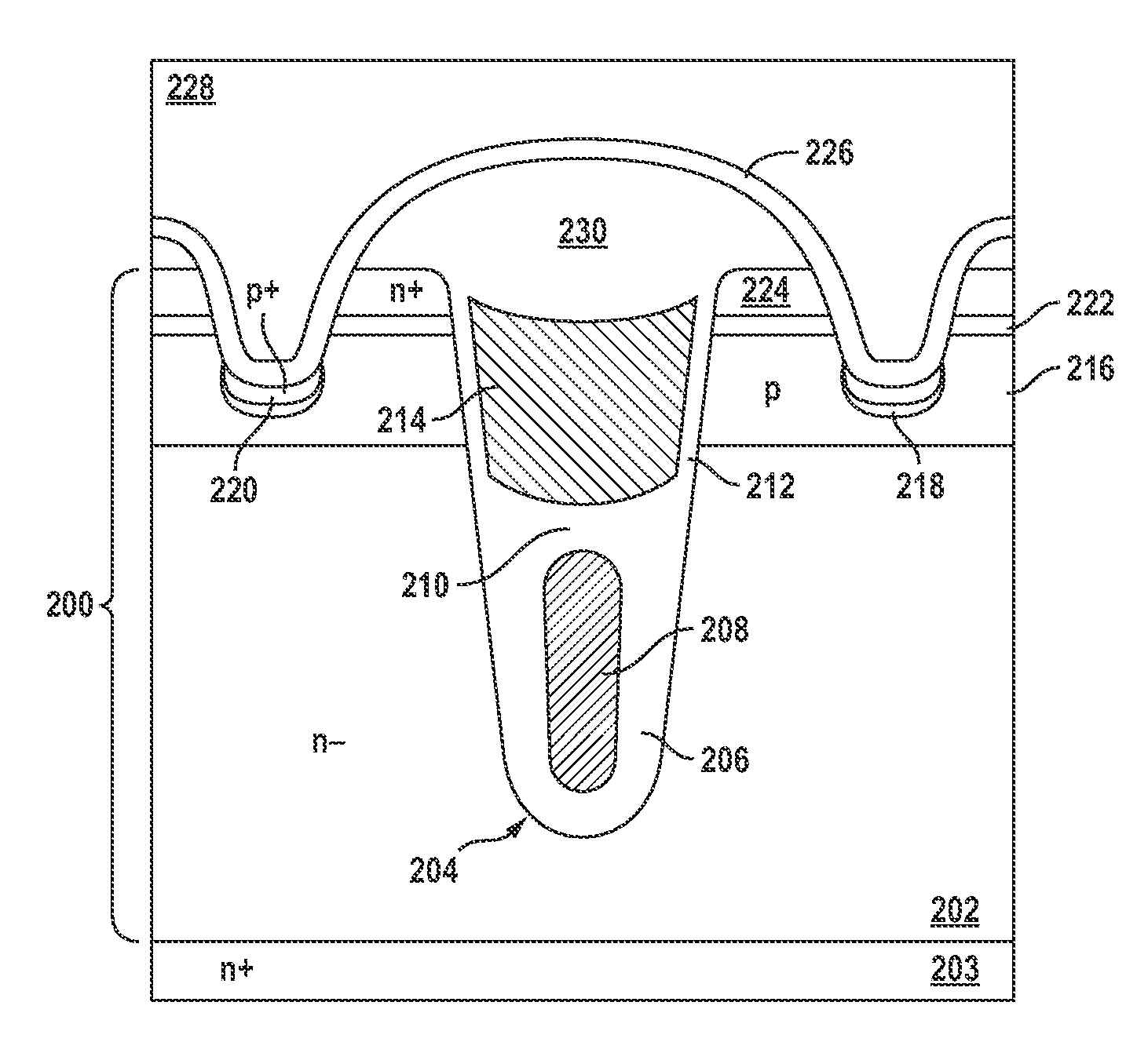
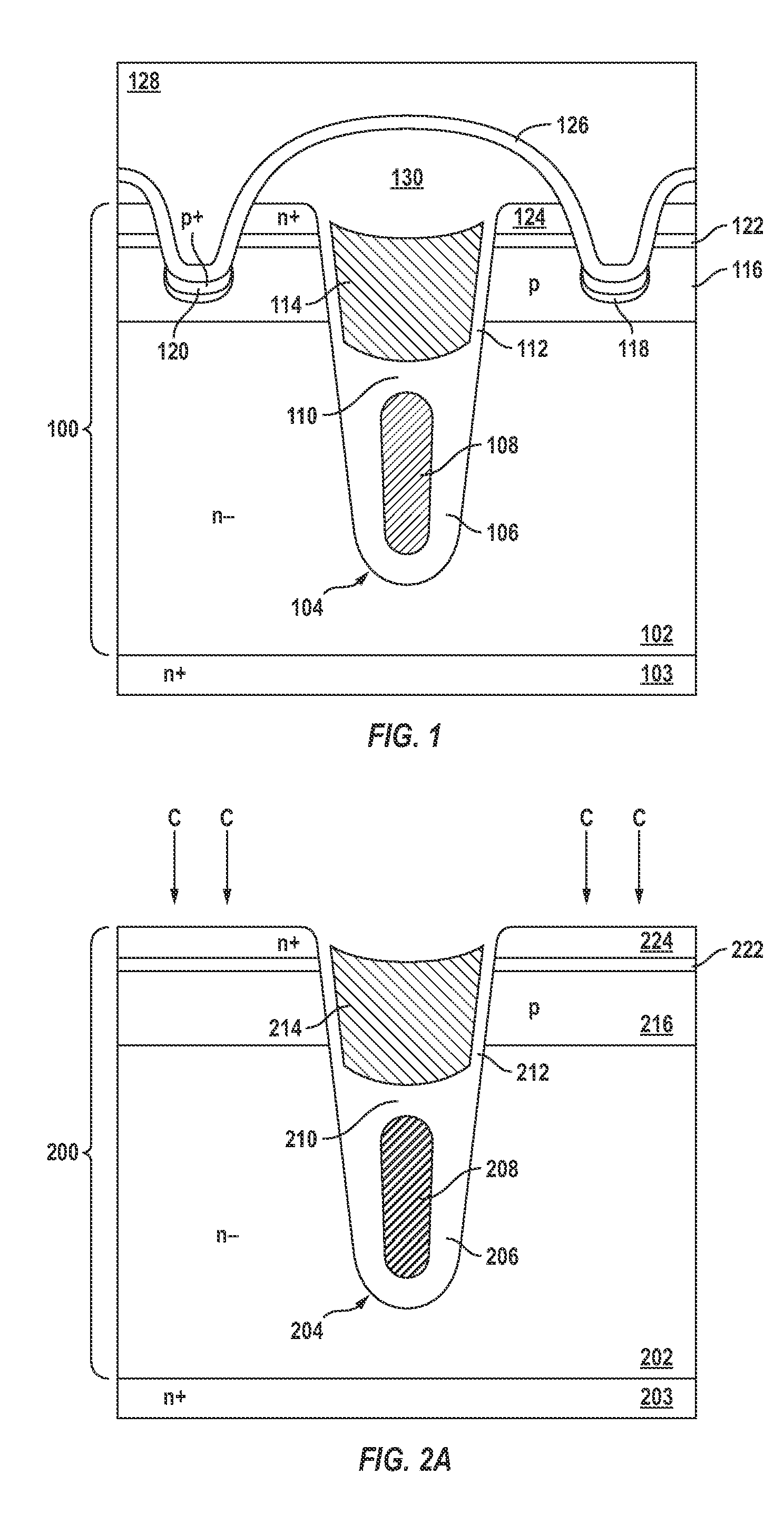
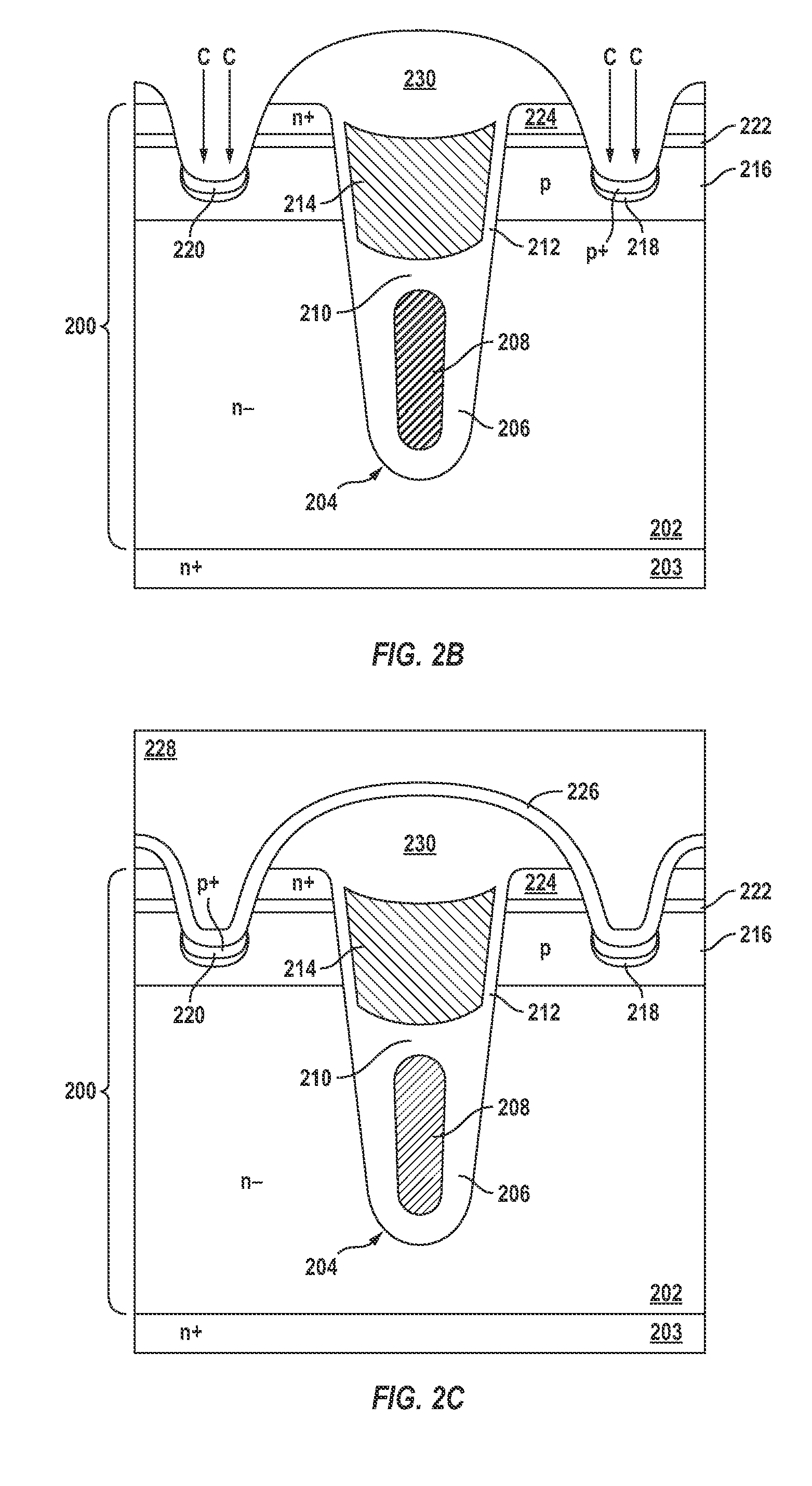
[0019]In accordance with embodiments of the present invention, FET structures with reduced out-diffusion from the heavy body and / or source regions are obtained using simple manufacturing processes. Some embodiments include FET structures with a diffusion barrier layer surrounding the heavy body region. Other embodiments include FET structures with a diffusion barrier layer extending between the source region and the well region. Each of these embodiments reduces out-diffusion of the heavy body and / or source dopants. These and other embodiments of the invention, as well as other features and advantages, are described in more detail below.

[0020]FIG. 1 shows a simplified cross-section view of a shielded gate trench FET structure with diffusion barrier regions, in accordance with an embodiment of the invention. As shown in FIG. 1, semiconductor region 100 includes source diffusion barrier regions 122 extending between n+ type source regions 124 and p-type well regions 116. Source diffus...


PUM


Abstract

A semiconductor structure comprises a drift region of a first conductivity type in a semiconductor region. A well region of a second conductivity type is over the drift region. A source region of the first conductivity type is in an upper portion of the well region. A heavy body region of the second conductivity type extends in the well region. The heavy body region has a higher doping concentration than the well region. A first diffusion barrier region at least partially surrounds the heavy body region. A gate electrode is insulated from the semiconductor region by a gate dielectric.

Description

BACKGROUND OF THE INVENTION[0001]The present invention relates in general to semiconductor technology, and more particularly, to structures and methods for reducing dopant out-diffusion from implant regions, such as source and heavy body regions, in power field effect transistors (FETs).[0002]In the design of FETs it is desirable to have a heavily doped body region that extends below the source region. This heavy body region provides a low resistance path around the source area to keep the well-source junction from becoming forward biased, thus preventing a parasitic bipolar transistor inherently present in power FETs from turning on. The ability of the transistor to avoid turning on this parasitic bipolar transistor is commonly referred to as ruggedness. A deep heavy body region also helps move the electric field and its breakdown current path away from the gate dielectric. Moving the electric field away from the gate dielectric reduces the possibility of damage by hot electrons.[0...

Claims


Application Information

Patent Timeline
Patent Type & Authority Patents(United States)
IPC IPC(8): H01L29/66
CPCH01L21/26506H01L29/0856H01L29/1095H01L29/161H01L29/407H01L29/41766H01L29/42368H01L29/456H01L29/66712H01L29/66727H01L29/66734H01L29/7802H01L29/7813H01L21/26513
Inventor PAN, JAMES
Owner SEMICON COMPONENTS IND LLC
Learn More