
Semiconductor device and manufacturing method thereof

a semiconductor and silicon dioxide technology, applied in the direction of solid-state devices, chemical vapor deposition coatings, coatings, etc., can solve the problems of reducing contact resistance, and reducing the efficiency of silicon dioxide film reforming

Inactive Publication Date: 2012-04-10
PS4 LUXCO SARL
View PDF5 Cites 5 Cited by
  • Summary
  • Abstract
  • Description
  • Claims
  • Application Information

AI Technical Summary

Benefits of technology

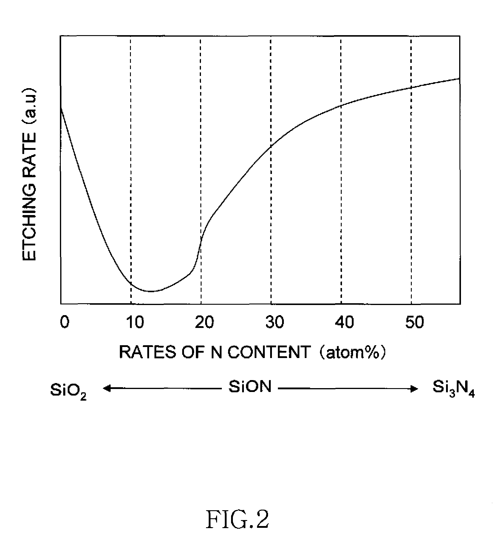
"The present invention relates to a semiconductor device and a manufacturing method thereof. The invention uses a SiON film with a specific composition to prevent the formation of NH3 and enhance the efficiency of reforming polysilazane into silicon dioxide film. The SiON film also has oxidation resistance to prevent the oxidation of metal films and reduce contact resistance between cell contacts and bit contacts. The technical effects of the invention include improved efficiency and reliability of semiconductor device manufacturing."

Problems solved by technology

With downsizing of elements, however, the STI trenches or the spaces between gate electrodes or bit lines have become narrower and accordingly it has become difficult to form the insulating films in these regions by the method mentioned above.
The silicon nitride film, however, has a great stress and is improper to be used as an interlayer insulating film.
However, the steaming may oxidize a metal film, a polycrystalline silicon film, or a silicon substrate in lower layers.
These problems can also occur in narrow regions between gate electrodes, STI regions, and the like.

Method used


Image

  • Semiconductor device and manufacturing method thereof
  • Semiconductor device and manufacturing method thereof
  • Semiconductor device and manufacturing method thereof

Examples


first modification

[First Modification]

[0071]According to the embodiment described above, in the LPCVD method using the mixed gas including dichlorosilane (SiH2Cl2) ammonia (NH3), and nitrous oxide (N2O), the composition ratios in the SiON films 210, 225, and 241 as the liner films are changed by changing the gas mixing ratio between NH3 and N2O to form the SiON films similar to the oxide film. However, the film forming method of the SiON film is not limited thereto. A modification of the film forming method of the SiON film is explained below.

[0072]FIG. 33 is a time chart for explaining a film forming method of a SiON film according to an ALD (Atomic Layer Deposition) method. As shown in FIG. 33, dichlorosilane (SiH2Cl2), ammonia (NH3), and ozone (O3) are used as film forming gases. In this modification, a pressure in a reaction chamber is constant.

[0073]The ALD method utilizes atom adsorption to a substrate, which is different from the CVD method that enables to produce SiO2 or Si3N4 in a free space...

second modification

[Second Modification]

[0077]FIG. 34 is a time chart for explaining another modification of the film forming method of the SiON film by the ALD method. As shown in FIG. 34, this modification is different from the method shown in FIG. 33 in that a step of vacuuming a reaction chamber is added between each of steps of injecting a film forming gas and each of N2 purging steps.

[0078]According to the film forming method shown in FIG. 34, while film formation time is longer than that in the modification shown in FIG. 33, content rates of Si, O, and N in a SiON film can be more precisely controlled.

third modification

[Third Modification]

[0079]In the embodiment described above, the example in which the coating and steaming of the polysilazane are each performed once to form the silicon dioxide film in the narrow groove-like regions has been described. A method of forming a silicon dioxide film in groove-like regions by using the polysilazane at two steps is explained here.

[0080]FIGS. 35A to 35D and 36A to 36D are schematic cross-sectional views for explaining modifications of a forming method of a silicon dioxide film by using the polysilazane in STI trenches and groove-like regions between gate electrodes, respectively.

[0081]A modification of the forming method of a silicon dioxide film in the STI trenches is explained with reference to FIGS. 35A to 35D. This modification is particularly applied suitably to cases where trenches have greater widths.

[0082]As shown in FIG. 35A, a pad oxide film 302 and a silicon substrate 301 are etched by using a silicon nitride film 303 having openings 304, there...


PUM

PropertyMeasurementUnit
depthaaaaaaaaaa
thicknessaaaaaaaaaa
thickaaaaaaaaaa

Abstract

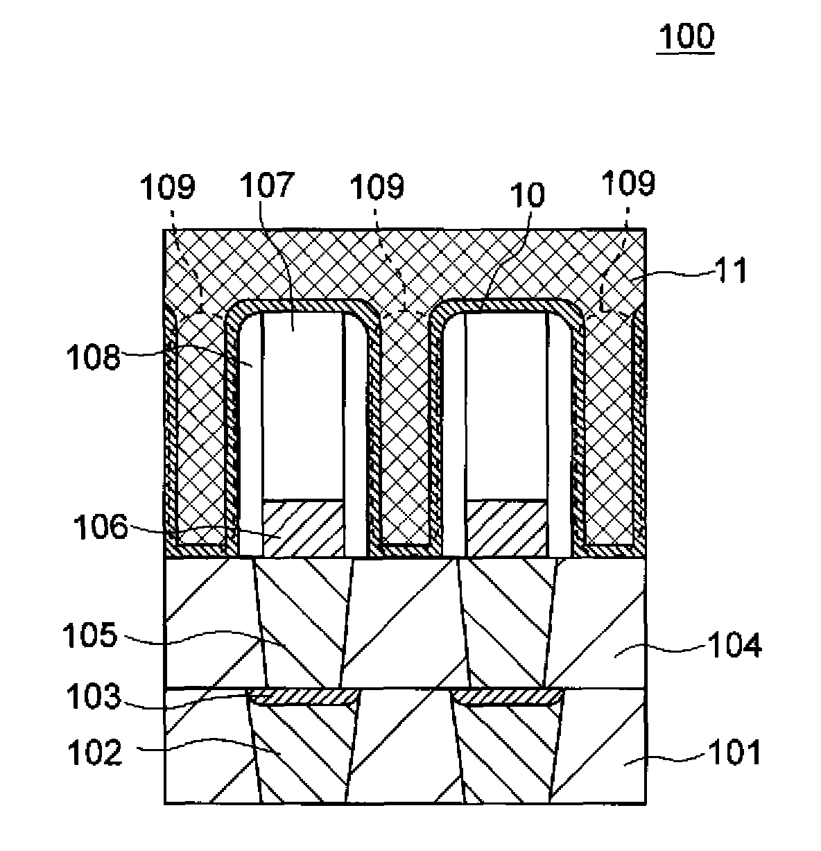
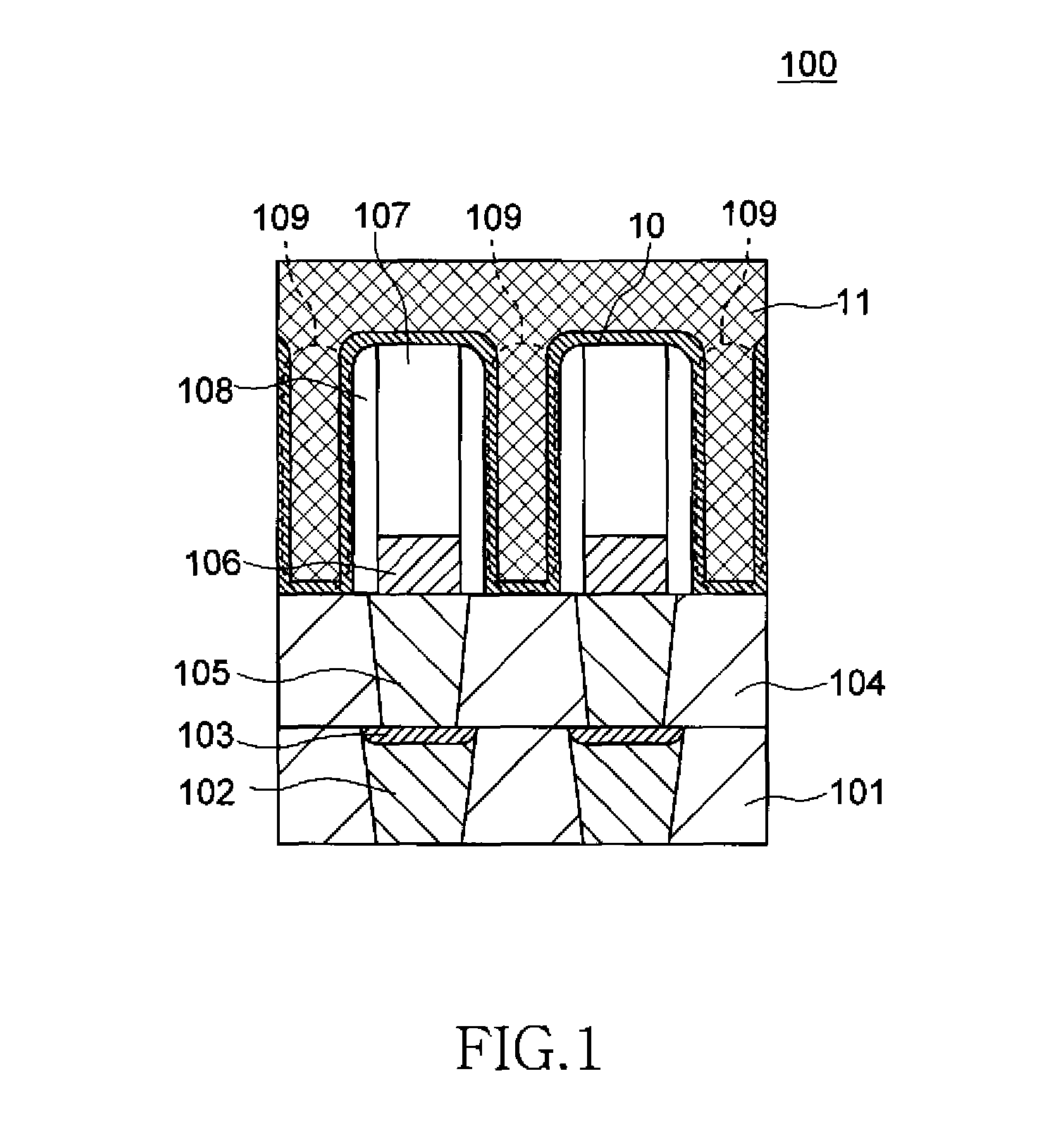
A semiconductor device includes groove-like regions that are formed between two adjacent bit lines among a plurality of bit lines each having upper and side surfaces covered with a cap insulating film and a side-wall insulating film, respectively, a SiON film that contains more O (oxygen) than N (nitrogen) and continuously covers inner surfaces of the groove-like regions, and a silicon dioxide film formed by reforming polysilazane and filled in the groove-like regions with the SiON film interposed therebetween.

Description

BACKGROUND OF THE INVENTION[0001]1. Field of the Invention[0002]The present invention relates to a semiconductor device and a manufacturing method thereof, and, more particularly relates to a semiconductor device having insulating films formed by using polysilazane and a manufacturing method of the semiconductor device.[0003]2. Description of Related Art[0004]Conventionally, in manufacturing process of a semiconductor device, insulating films in narrow regions such as an STI (Shallow Trench Isolation) trench and a space between gate electrodes or bit lines are formed by means of a HDP-CVD (High Density Plasma-Chemical Vapor Deposition) method, depositing BPSG (Boron Phosphorus Silicon Glass) and reflowing the deposited BPSG, or the like. With downsizing of elements, however, the STI trenches or the spaces between gate electrodes or bit lines have become narrower and accordingly it has become difficult to form the insulating films in these regions by the method mentioned above.[0005]...

Claims


Application Information

Patent Timeline
Patent Type & Authority Patents(United States)
IPC IPC(8): H01L21/70
CPCC23C16/308C23C16/45525H01L21/0214H01L21/02164H01L21/02211H01L21/02222H01L21/02271H01L21/0228H01L21/02282H01L21/02337H01L21/3105H01L21/3125H01L21/3141H01L21/3145H01L21/76232H01L21/76834H01L21/76837H01L27/10876H01L27/10885H01L27/10888H01L29/66621H01L27/0207H10B12/053H10B12/485H10B12/482H01L21/02274H01L21/0217H01L21/76H01L21/31
Inventor MATSUDA, YOHMIYATA, KYOKO
Owner PS4 LUXCO SARL
Learn More