Switching element and manufacturing method thereof
a technology of switching element and manufacturing method, which is applied in the field of switching element, can solve the problems of difficult effective suppression and difficult effective control of the switching phenomenon of the active layer by the gate bias voltage, and achieve excellent and stable transistor characteristics, improve interaction
- Summary
- Abstract
- Description
- Claims
- Application Information
AI Technical Summary
Benefits of technology
Problems solved by technology
Method used
Image
Examples
first embodiment
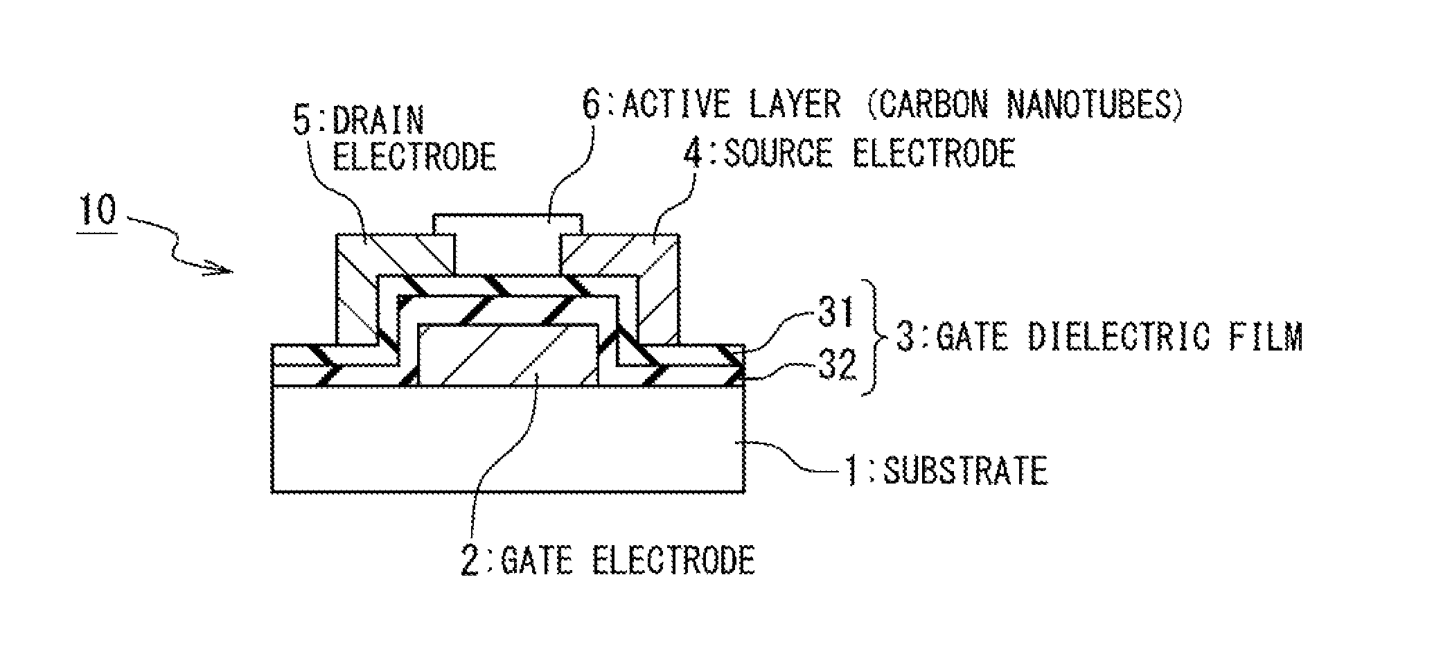
[0036]The configuration of a switching element 10 in a first embodiment of the present invention will be described referring to the Drawings.
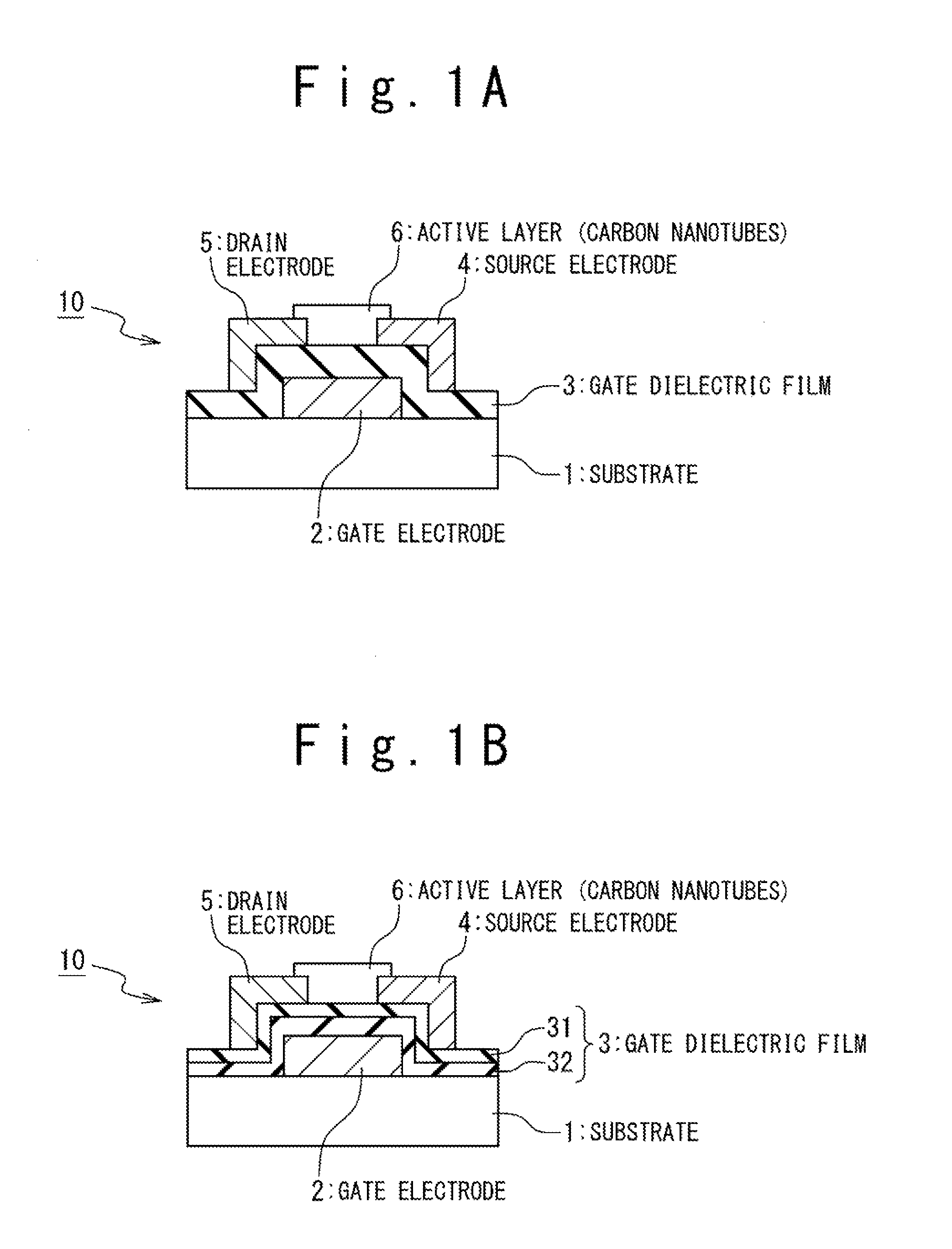
[0037]FIG. 1A is a schematic sectional view showing the configuration of the switching element 10 according to the present invention. As shown in FIG. 1A, the switching element 10 includes: a supporting substrate 1; a gate electrode 2 formed on the supporting substrate 1; a gate dielectric film 3 provided on the supporting substrate 1 so as to cover the gate electrode 2; source and drain electrodes 4 and 5 which are provided on the gate dielectric film 3 at a distance therebetween corresponding to the channel length; and an active layer 6 provided in contact with all of the gate dielectric film 3, the source electrode 4 and the drain electrode 5. As described above, the switching element 10 in the present embodiment is a so-called bottom-contact type thin film transistor.
[0038]The material of the supporting substrate 1 is not specifically limit...
second embodiment
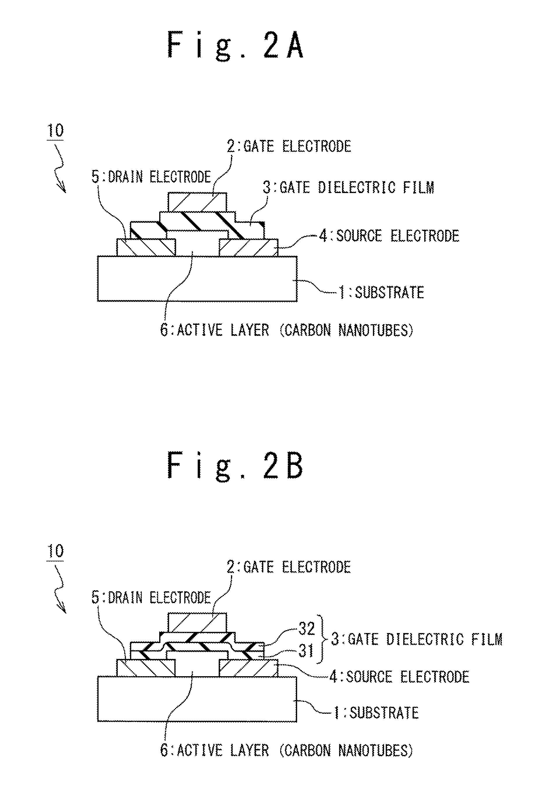
[0069]Subsequently, a description is given of a second embodiment of the present invention. FIG. 2A is a schematic sectional view of a switching element 10 of this embodiment. As shown in FIG. 2A, the switching element 10 of this embodiment includes: a supporting substrate 1; source and drain electrodes 4 and 5 which are disposed on the supporting substrate 1 with a distance therebetween corresponding to the channel length; an active layer 6 formed so as to be in contact with these electrodes, a gate dielectric film 3 formed on the source electrode 4, the drain electrode 5 and the active layer 6 and the gate electrode 2 formed on the gate dielectric film 3. That is, the switching element 10 according to the present embodiment has a top-contact structure in which the gate electrode 2 exists on an opposite side to the supporting substrate 1 across the active layer 6. Since materials for the supporting substrate 1, the source electrode 4, the drain electrode 5, the active layer 6, the ...
embodiment 1
[0074]A description is given of a method of manufacturing the switching elements 10 of Embodiment 1. The structure of the switching elements 10 of Embodiment 1 is the same as that shown in FIG. 1A. First, a polyethylene naphthalate substrate having a thickness of 0.5 mm was prepared as the supporting substrate 1 and an aluminum film of 100 nm was formed as the gate electrode 2 on the supporting substrate 1 by using a shadow mask according to the sputtering method. Next, a xylene solution of polystyrene (non-conjugated polymer having a aromatic group in the side chain) was applied as the gate dielectric film 3 by a spin coat method and dried at 120° C. to form a film having a thickness of 100 nm. Gold was deposited thereon as the source and drain electrodes 4 and 5 by a vacuum deposition method through a shadow mask so that the source and drain electrodes 4 and 5 have a thickness of 60 nm. In this electrode structure thus formed, the channel width and length were 200 μm and 50 μm, re...
PUM
| Property | Measurement | Unit |
|---|---|---|
| thickness | aaaaa | aaaaa |
| thickness | aaaaa | aaaaa |
| thickness | aaaaa | aaaaa |
Abstract
Description
Claims
Application Information
 - R&D
- Intellectual Property
- Life Sciences
- Materials
- Tech Scout
- Unparalleled Data Quality
- Higher Quality Content
- 60% Fewer Hallucinations
Browse by: Latest US Patents, China's latest patents, Technical Efficacy Thesaurus, Application Domain, Technology Topic, Popular Technical Reports.
© 2025 PatSnap. All rights reserved.Legal|Privacy policy|Modern Slavery Act Transparency Statement|Sitemap|About US| Contact US: help@patsnap.com


