Determining macro blocks terminal for integrated circuit layout

a technology of integrated circuit layout and terminals, which is applied in the direction of cad circuit design, program control, instruments, etc., can solve the problems of deteriorating the wiring property of the entire lsi, unable to achieve optimal results, and increasing the length, so as to suppress the deterioration of the wiring delay time and improve the wiring property of the semiconductor integrated circuit.

Inactive Publication Date: 2012-02-14
NEC CORP
View PDF11 Cites 2 Cited by
  • Summary
  • Abstract
  • Description
  • Claims
  • Application Information

AI Technical Summary

Benefits of technology

[0031]An exemplary object of the present invention is to provide an integrated circuit layout design supporting device which can avoid bypass wirings to shorten the wiring length when using a plurality of same-type macro blocks.
[0034]As an exemplary advantage according to the invention, regarding the wiring layout processing inside and outside a plurality of macro blocks including a plurality of same-type macro blocks, it is possible to design layout by shortening all the wirings connected to the macro terminals while securing the necessary macro block area without performing unnecessary processing such as provisional layout and schematic wiring processing, offset processing, or clamp processing, and without forming unnecessary elements. Therefore, it is possible to avoid bypass wirings (detour routing of the wirings) and improve the wiring property of the semiconductor integrated circuit so as to suppress deterioration in the wiring delay time.

Problems solved by technology

When a plurality of same-type macro blocks are used on the chip, an optimum result cannot be achieved in some cases, because the circuit delay in a system LSI in timing designing cannot be set within a range of delay required for achieving a normal operation, due to the wiring property between the macro blocks depending on the layout regarding the same-type macro blocks and other different types of macro blocks formed in the surroundings thereof.
Therefore, the wiring length is increased, which results in deteriorating the wiring property of the entire LSI and deteriorating the wiring delay time.
Further, in Patent Document 1, it is necessary to change the terminal positions, wirings, and the like again after performing the schematic wiring processing, which results in increasing the number of unnecessary processing steps.
Thus, when a plurality of same-type macro blocks are to be used, the uniformity of each macro block cannot be secured.
Furthermore, it is necessary to perform correction after provisional layout is performed once by the provisional layout device, so that the number of unnecessary processing steps is increased.
This increases not only the number of processing steps but also the amount of calculation for rotating or moving the macro blocks as well as the time required for the processing.
Further, since bypass wirings are formed within the macro blocks, the total wiring length of the chip as a whole can not be formed short.
Thus, there is required more time for the processing.
Thus, there is required still more time and effort.
Thus, it requires time and effort for performing the processing, and the number of processing steps is increased.
Further, the clamp cells as well as the wirings for connecting the unused terminals and the clamp cells CS need to be provided outside the area of the macro block 1010, thereby increasing the number of unnecessary elements and wirings.
This causes delay in the processing speed and increase in the power consumption of the entire chip.
Thus, the actual functioning macro area cannot be utilized effectively.
To provide such function parts used exclusive for connection other than those functioning originally as macro circuits in the macro blocks 1010 results in useless increase in the number of elements and wirings, which causes delay in the operation speed of the entire chip.

Method used


Image

  • Determining macro blocks terminal for integrated circuit layout
  • Determining macro blocks terminal for integrated circuit layout
  • Determining macro blocks terminal for integrated circuit layout

Examples


first exemplary embodiment

(Overall Structure of Integrated Circuit Layout Design Supporting Device)

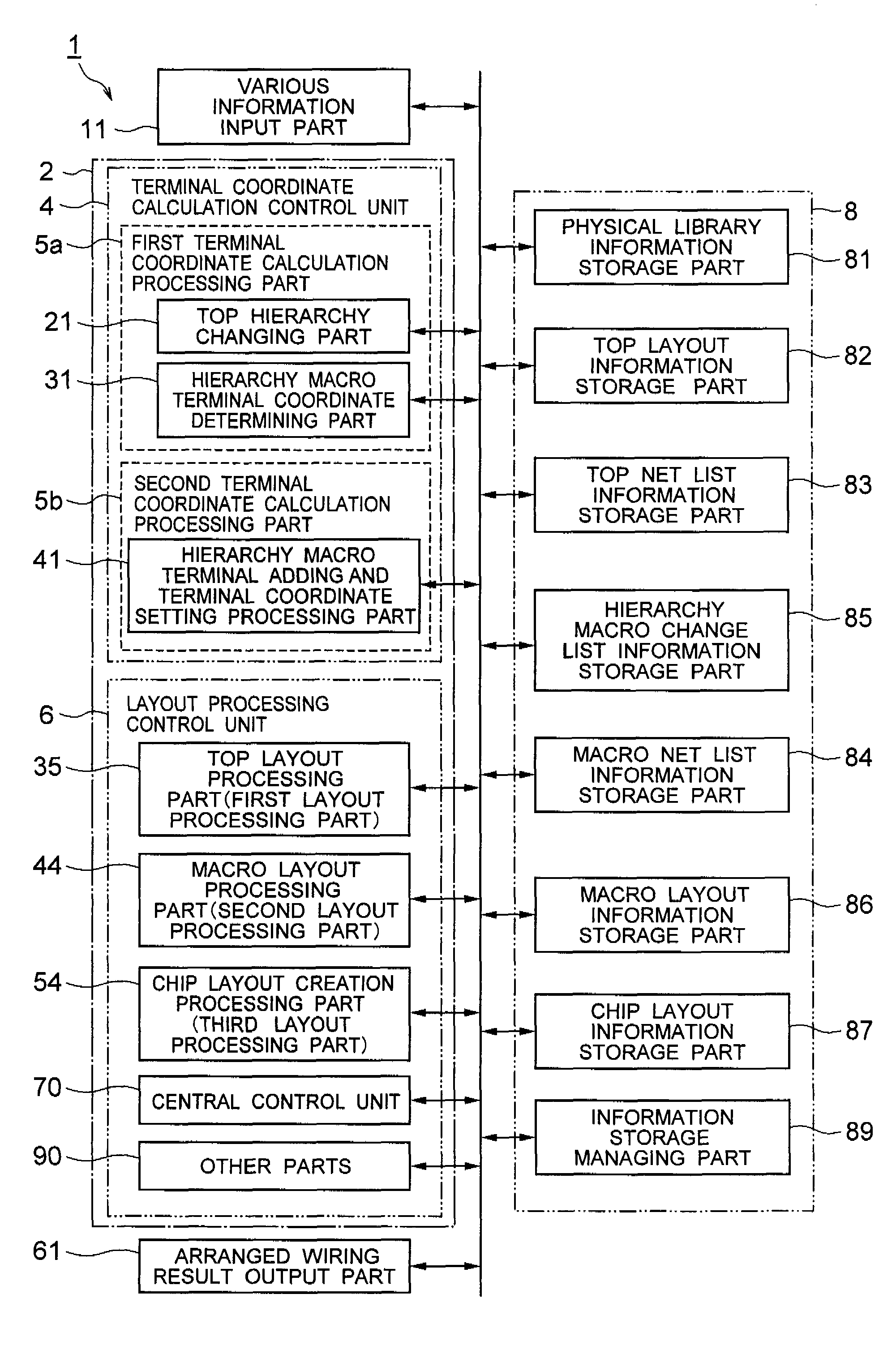
[0072]First, the overall structure of an integrated circuit layout design supporting device according to the present invention will be described by referring to FIG. 1. FIG. 1 is a block diagram showing a schematic structure of the entire LSI layout design supporting device according to this exemplary embodiment.

[0073]A layout design supporting device 1 for an integrated circuit (for example, LSI) according to the exemplary embodiment is an information processor (computer) used by a user for designing an integrated circuit. As shown in FIG. 1, the layout design supporting device 1 includes: a various information input part 11 for inputting various types of information; a storage unit 8 as an accumulating processing part which stores and performs accumulating processing of information that is registered in advance and information inputted by the user (layout designer) through operations; an arranged wiring resul...

second exemplary embodiment

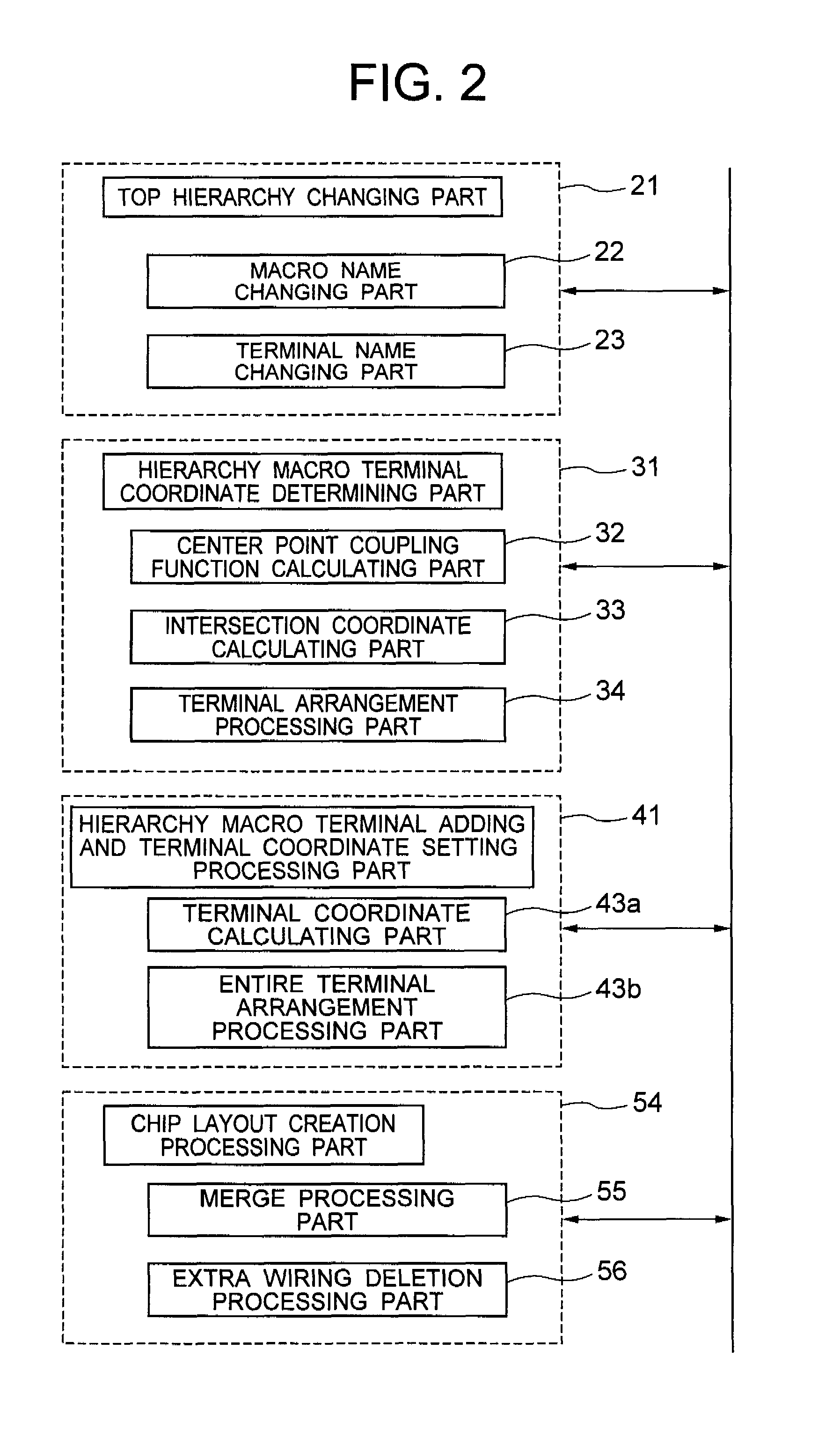
[0242]Next, a second exemplary embodiment according to the present invention will be described by referring to FIG. 27-FIG. 30. Explanations of substantially the same structures as those of the first exemplary embodiment will be omitted, and only different points will be described hereinafter. FIG. 8 is a block diagram showing an example of the second exemplary embodiment of the layout design supporting device according to the present invention. The structures of the layout design supporting device of this exemplary embodiment is different from the structures of the layout design supporting device of the first exemplary embodiment described above in regards to the structure of the hierarchy macro terminal coordinate determining part.

[0243]That is, the above-described first exemplary embodiment describes the method which obtains the intersection part between the coupling lines that connect center points of each macro block and the boundary line of each macro block for calculating the...

modification examples

(Various Modification Examples)

[0253]While the LSI layout design supporting device and LSI layout designing method according to the present invention have been described by referring to some of the specific exemplary embodiments, various modifications to the exemplary embodiments of the present invention illustrated herein are possible without departing from the spirit and scope of the present invention. For example, there has been described the case of using a linear function (straight line form) as the coupling function for calculating the optimum positions of the macro terminals in the first exemplary embodiment. However, it is not limited only to that. As shown in FIG. 31, the coupling function may be a cubic function that goes through three points, or a free-form curve that goes through two points.

[0254]If the function is in a linear form when the macro blocks are in the layout of FIG. 31, the intersection part between the coupling function L1 and the boundary line of the macro...


PUM


Abstract

Provided is an integrated circuit layout design supporting device which can reduce the wiring length by avoiding bypass wirings when a plurality of same-type macro blocks are used. The integrated circuit layout design supporting device includes a terminal coordinate calculation control unit and a layout processing control unit. The terminal coordinate calculation control unit considers the plurality of same-type macro blocks included in a plurality of types of macro blocks as each of different types of macro blocks, and calculates the optimum coordinate positions of each macro terminal of each macro block. The layout processing control unit performs various types of wiring layout processing related to each of the macro terminals based on each of the macro terminal positions calculated by the terminal coordinate calculation control unit.

Description

CROSS-REFERENCE TO RELATED APPLICATION[0001]This application is based upon and claims the benefit of priority from Japanese patent application No. 2007-053302, filed on Mar. 2, 2007, the disclosure of which is incorporated herein in its entirety by reference.BACKGROUND OF THE INVENTION[0002]1. Field of the Invention[0003]The present invention relates to an integrated circuit layout design supporting device, an integrated circuit layout design supporting method, a program, and a data structure thereof.[0004]2. Description of the Related Art[0005]For designing layout of a large-scaled integrated circuit (for example, LSI), widely used is a method which enables a designing period to be shortened by dividing a chip into pieces of a design unit called a macro (macro block) by a hierarchy layout style and performing layout processing of each macro block in parallel.[0006]In such layout designing of an LSI that uses a plurality of macro blocks including a same function, it is considered to...

Claims


Application Information

Patent Timeline
Patent Type & Authority Patents(United States)
IPC IPC(8): G06F17/50
CPCG06F30/39
Inventor GOTOU, TAKASHI
Owner NEC CORP
Why Eureka
Try Eureka