Mounting board and method of producing the same
a technology of mounting board and mounting plate, which is applied in the manufacture of final products, electrical apparatus construction details, and semiconductor/solid-state device details, etc., can solve the problems of poor conductivity, local cell corrosion, galvanic corrosion, etc., and achieve the effect of improving connection reliability, reducing distance between solder pieces, and stable conduction
- Summary
- Abstract
- Description
- Claims
- Application Information
AI Technical Summary
Benefits of technology
Problems solved by technology
Method used
Image
Examples
first embodiment
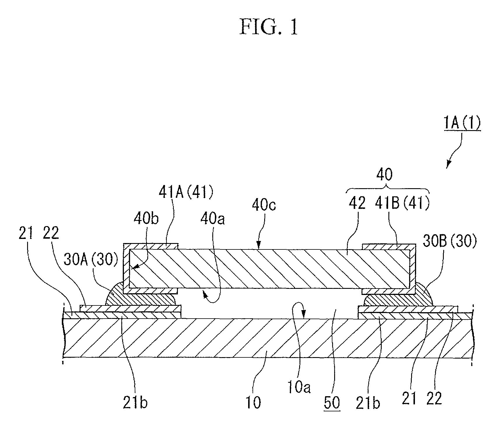
[0064]FIG. 1 is a cross-sectional view schematically showing an exemplary mounting board according to the invention.
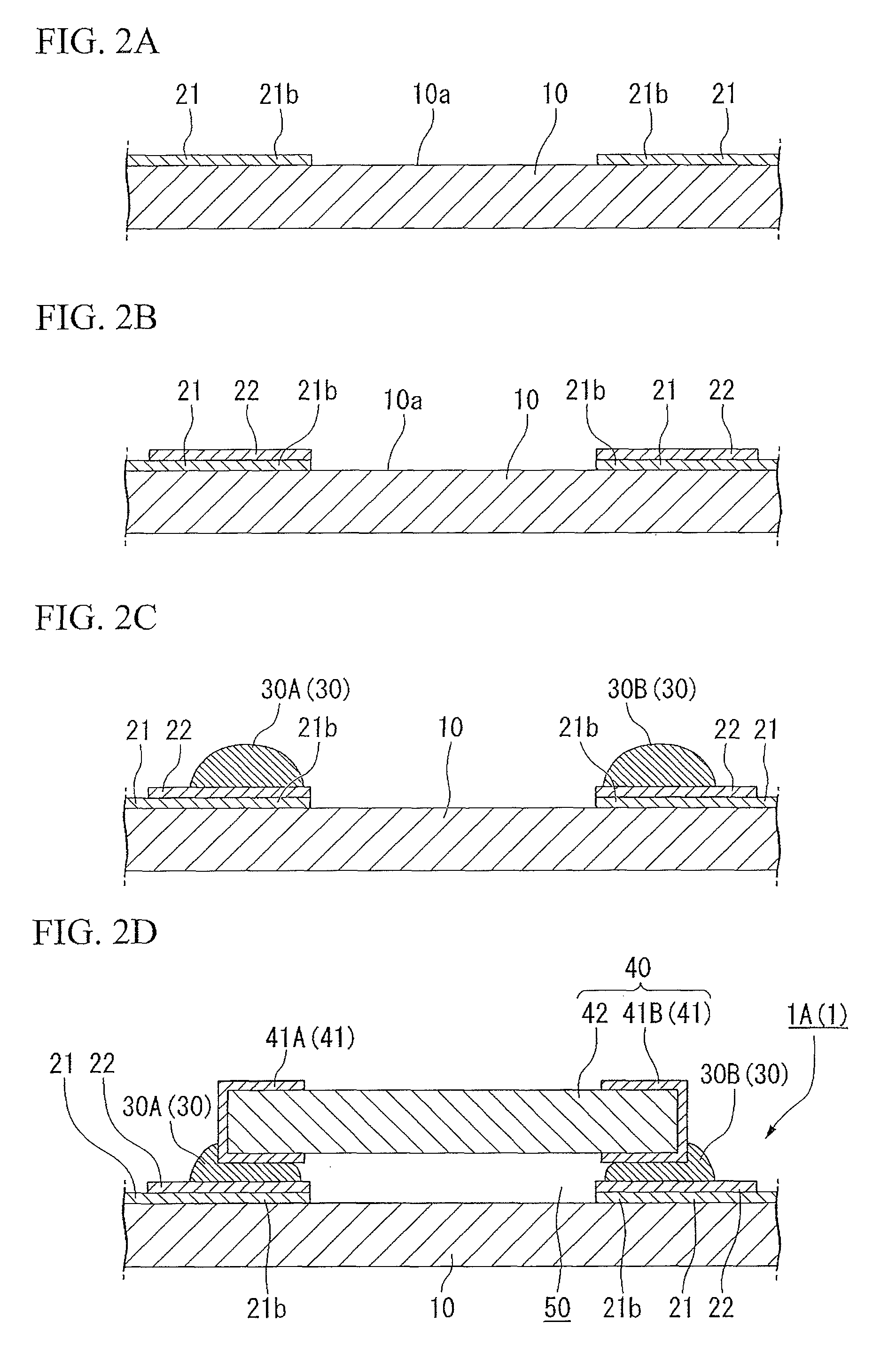
[0065]A mounting board 1 of the invention schematically includes: an insulative base 10; a plurality of first conductive elements 21 provided on the insulative base 10 and having lands 21b; a plurality of second conductive elements 22 disposed on the lands 21b; a plurality of solder pieces 30 each disposed on each of the second conductive elements 22; and an electronic component 40 which includes electrode sections 41 each contacting each of the solder pieces 30. The first conductive elements 21 are made from a first element that contains at least silver. The second conductive elements 22 are made from a second element that contains at least copper. The solder pieces 30 are made from a third element that contains at least tin.
[0066]Hereinafter, each component will be described in detail.
[0067]The insulative base 10 is made from resin, glass or other materials, among wh...
modified embodiment
[0085]FIGS. 3A, 3B and 3C schematically show an exemplary mounting board 1B according to a modified embodiment of the present embodiment. FIG. 3A is a cross-sectional view and FIG. 3B is a plan view of the mounting board 1B. FIG. 3C is a plan view of vicinities of lands 21b.
[0086]In the mounting board 1B of the modified embodiment, second conductive elements 22 are larger than the lands 21b of first conductive elements 21.
[0087]The radius R2 of the second conductive elements 22 is larger than the radius R1 of the lands 21b of the first conductive elements 21 by a as shown in FIG. 3C. Preferably, a is larger than a degree of printing alignment accuracy during production of the second conductive elements 22, and is not less than 0.2 mm, for example. The second conductive elements 22 are not necessarily formed concentric with the lands 21b, as shown in FIGS. 3A to 3C.
[0088]Thickness of the second conductive elements 22 is suitably adjusted depending on the electronic equipment in whic...
second embodiment
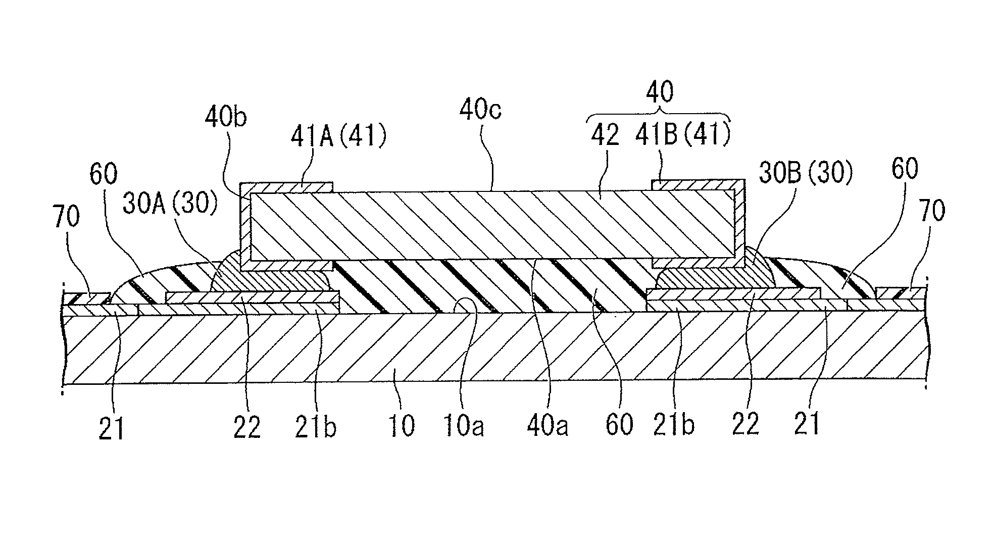
[0090]FIG. 4A is a cross-sectional view schematically showing a mounting board 1C according to a second embodiment of the invention. The mounting board 1C of the present embodiment differs from the mounting board 1A of the first embodiment in that resin 60 is provided in space 50 at least between an electronic component 40 and an insulative base 10. Also in the present embodiment, first conductive elements 21 are covered with resist 70 such that areas other than lands 21b of the first conductive elements 21 and vicinities thereof are not exposed.
[0091]The resin 60 is not particularly limited so long as it is thermosetting and is used as a non-conductive adhesive agent. Examples of the resin 60 may include epoxy resin and acrylic resin.
[0092]The resin 60 is disposed in the space 50 between the electronic component 40 and the insulative base 10 so as to adhere to the electronic component 40 and the insulative base 10, thereby improving fixing strength of the electronic component 40 to...
PUM
| Property | Measurement | Unit |
|---|---|---|
| soldering temperature | aaaaa | aaaaa |
| temperature | aaaaa | aaaaa |
| thickness | aaaaa | aaaaa |
Abstract
Description
Claims
Application Information
 - R&D
- Intellectual Property
- Life Sciences
- Materials
- Tech Scout
- Unparalleled Data Quality
- Higher Quality Content
- 60% Fewer Hallucinations
Browse by: Latest US Patents, China's latest patents, Technical Efficacy Thesaurus, Application Domain, Technology Topic, Popular Technical Reports.
© 2025 PatSnap. All rights reserved.Legal|Privacy policy|Modern Slavery Act Transparency Statement|Sitemap|About US| Contact US: help@patsnap.com


