


Quick Research
Generate reliable direction feasibility study reports for your R&D in just a few steps.

Technical Q&A
Discover and master advanced knowledge NOW. Basics, ideas, possibilities, all at once.

Find Solutions
As an expert in R&D theories, this can generate solutions to your technical problems instantly.

Evaluate Feasibility
Analyze your overall solution with one click, know your potential R&D risks in advance.

Monitor Landscape
Get weekly tech updates, stay abreast of the latest tech innovations and key insights.
Shift register circuit and display panel
A shift register and circuit technology, applied in static memory, digital memory information, instruments, etc., can solve problems such as increased power consumption, abnormal output signals, etc., and achieve the effect of simple structure and low cost
- Summary
- Abstract
- Description
- Claims
- Application Information
AI Technical Summary
Problems solved by technology
Method used
Image

Examples
Embodiment approach 1
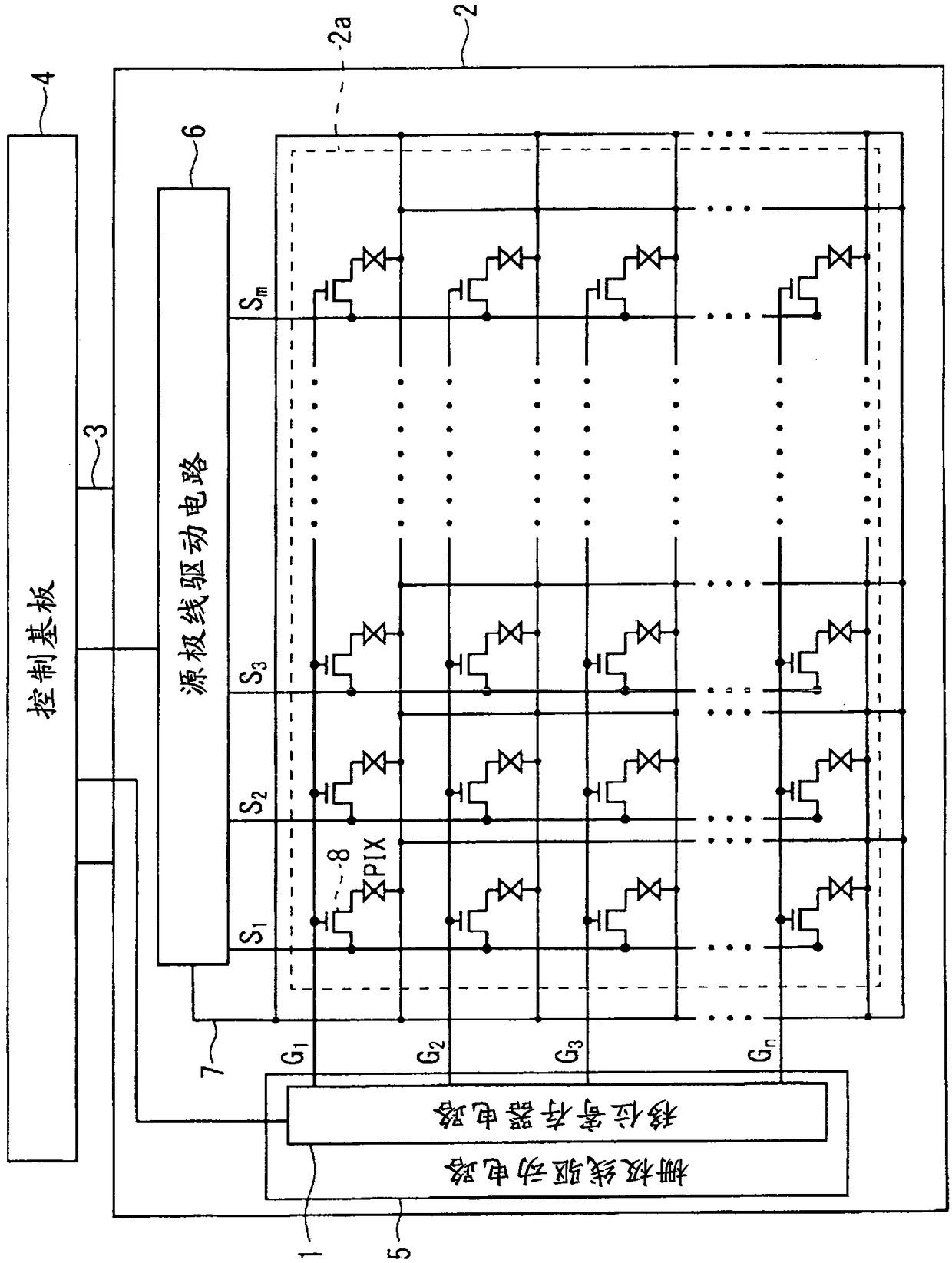
[0042] figure 1 It is a diagram showing the configuration of the liquid crystal display device in the first embodiment. Such as figure 1 As shown, the liquid crystal display device includes a display panel 2 , a flexible printed substrate 3 , and a control substrate 4 .
[0043] The display panel 2 is an active matrix display panel. In the display panel 2, a display region 2a, a plurality of gate lines (scanning signal lines), a plurality of source lines (data signal lines), gate The electrode line driving circuit 5 and the source line driving circuit 6 are an active matrix type display panel.
[0044] In the display area 2a, a plurality of pixels PIX are arranged in a matrix. The pixel PIX includes a TFT 8 as a pixel selection element, a liquid crystal capacitor, and an auxiliary capacitor. The gate of TFT8 is connected to the gate line, and the source of TFT8 is connected to the source line. The liquid crystal capacitor and the auxiliary capacitor are connected to the ...
Embodiment approach 2
[0132] In the unit shift register SR in Embodiment 1, the first transistor Q1 and the transistor Q5 for a back gate are normally closed in an initial state. On the other hand, in the unit shift register SR in the second embodiment, the back gate transistor Q5 is normally open from the initial state.
[0133] Figure 10 It is a graph showing the characteristics of the drain-source current when the transistor Q5 for a back gate is normally closed (Embodiment 1) and normally open (Embodiment 2). Such as Figure 10 As shown, when the back gate transistor Q5 is normally closed, almost no current flows between the drain and the source when the gate and the source are at the same potential. On the other hand, when the back gate transistor Q5 is normally open, a current flows between the drain and the source even if the gate and the source are at the same potential.
[0134] In particular, it is known that a TFT using an oxide semiconductor tends to be normally on depending on the ...
Embodiment approach 3
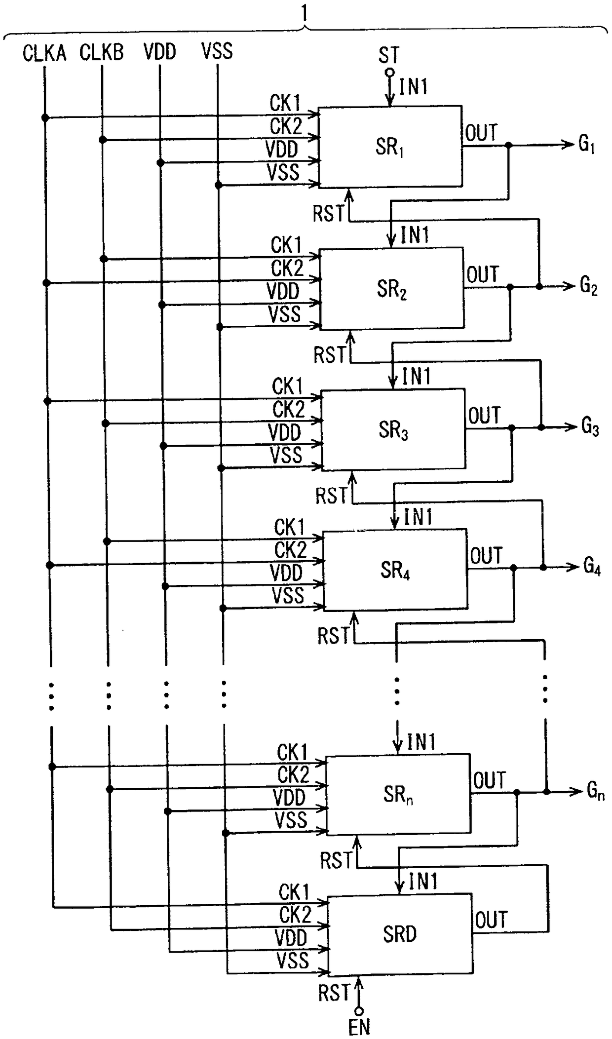
[0148] Figure 15 It is a figure which shows the structure of the unit shift register SR in this Embodiment 3. In the back gate voltage generation circuits 300 and 300A of Embodiments 1 and 2 ( Figure 4 , 11 ) shows the case where the back gate node N2 is connected only to the back gate capacitive element C2. On the other hand, the back gate voltage generation circuit 300B of Embodiment 3 further includes a capacitive element C3 for voltage division.
[0149] Such as Figure 15 As shown, the capacitive element C3 for voltage division is connected between the node N2 for the back gate and the first power supply terminal S2 having the potential VSS. The back gate node N2 is connected between the back gate capacitive element C2 and the voltage dividing capacitive element C3.
[0150] In the third embodiment, since the structure of the liquid crystal display device and the structure of the shift register circuit 1 are different from those of the first embodiment ( figure 1 ...
PUM
 Abstract
Description
Claims
Application Information
 - R&D Engineer
- R&D Manager
- IP Professional
- Industry Leading Data Capabilities
- Powerful AI technology
- Patent DNA Extraction
Browse by: Latest US Patents, China's latest patents, Technical Efficacy Thesaurus, Application Domain, Technology Topic, Popular Technical Reports.
© 2024 PatSnap. All rights reserved.Legal|Privacy policy|Modern Slavery Act Transparency Statement|Sitemap|About US| Contact US: help@patsnap.com