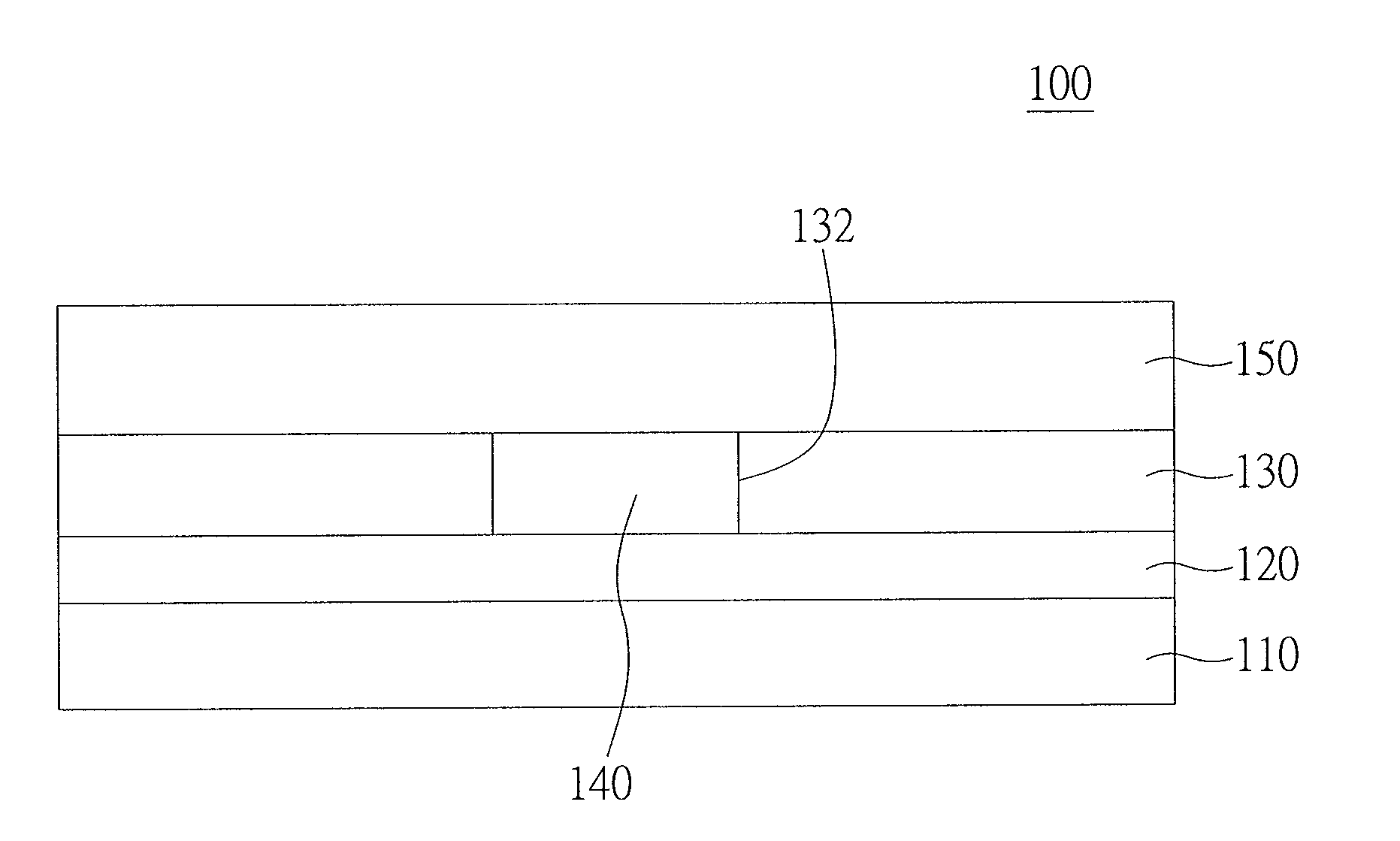
Phase-change material, memory unit and method for electrically storing/reading data
a phase-change memory and memory unit technology, applied in the direction of vacuum evaporation coating, instruments, semiconductor/solid-state device details, etc., can solve the problems of difficult control of the characteristics of the above storage unit, low resistance in the memory unit of a phase-change memory (pram), and high loss of current of the unit, so as to avoid incomplete reset
- Summary
- Abstract
- Description
- Claims
- Application Information
AI Technical Summary
Benefits of technology
Problems solved by technology
Method used
Image
Examples
examples
Preparative Example
[0038]One silica glass substrate of 1 cm2 processed with basic cleaning steps is ready for use. The indium oxide powder of 99.999% in purity and the gallium oxide powder of 99.999% in purity (Aldrich Chemical Co.) are loaded respectively in a capped tantalum boat smeared with aluminum oxide to form a substrate for vapor deposition process, and the substrate is then placed into an evaporation chamber and is processed by means of a mechanical pump and a turbo pump as the bottom pressure reaches 5×10⁻⁶ torr. In the vapor deposition process, oxygen and nitrogen are continuously inletted at the amount of 20 standard cubic centimeter per minute (20 sscm), and the pressure inside the chamber is controlled at 8×10⁻³ torr by means of a throttle valve. The temperature is maintained below 80° C., and the evaporation rate is maintained between 0.9 and 1.2 nm / sec so that the In—Ga—N—O thin film in an amorphous state is obtained.
[0039]The phase-change material thin film is heat...
example 3
[0043]A layer of the phase-change material of Ge—O—N is formed on the bottom substrate and has a thickness of 20 μm. Then, a passivation structure of silicon dioxide and a metal cushion at the top are formed so as to obtain a memory unit sample. A current-voltage graph of the memory unit sample is illustrated in FIG. 5. The resistance at an amorphous state is 402 kΩ, and the resistance at a crystalline state is 80Ω. The critical current for phase change is about 2 mA.
example 4
[0044]A layer of the phase-change material of In—O—N is formed on the bottom substrate and has a thickness of 20 μm. Then, a passivation structure of silicon dioxide and a metal cushion at the top are formed so as to obtain a memory unit sample. A current-voltage graph of the memory unit sample is illustrated in FIG. 6. The resistance at an amorphous state is 17 kΩ, and the resistance at a crystalline state is 115Ω. The critical current for phase change is 0.16 mA.
PUM
| Property | Measurement | Unit |
|---|---|---|
| temperature | aaaaa | aaaaa |
| temperature | aaaaa | aaaaa |
| thickness | aaaaa | aaaaa |
Abstract
Description
Claims
Application Information
 - R&D
- Intellectual Property
- Life Sciences
- Materials
- Tech Scout
- Unparalleled Data Quality
- Higher Quality Content
- 60% Fewer Hallucinations
Browse by: Latest US Patents, China's latest patents, Technical Efficacy Thesaurus, Application Domain, Technology Topic, Popular Technical Reports.
© 2025 PatSnap. All rights reserved.Legal|Privacy policy|Modern Slavery Act Transparency Statement|Sitemap|About US| Contact US: help@patsnap.com


